Showing Spotlights 265 - 272 of 315 in category All (newest first):
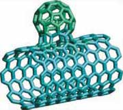 Carbon comes in many different forms, from the graphite found in pencils to the world's most expensive diamonds. While diamonds might be very popular among ladies, the two most celebrated carbon materials among nanotechnology scientists are fullerenes and carbon nanotubes. What makes them so interesting are the many advantageous properties that they exhibit. Despite the similarities between these two forms of carbon, there have been very few attempts to physically merge them. An international research group, led by a Finnish team, now has discovered a novel hybrid material that combines fullerenes and single-walled carbon nanotubes (SWCNTs) into a single structure in which the fullerenes are covalently bonded to the outer surface of the SWCNTs. In this newly discovered material, that the researchers termed NanoBuds, the fullerene molecules are attached to the outside surface of the carbon nanotubes, just like buds on the branch of a tree - hence the name - and can be made in a simple one-step process. These NanoBuds have been shown to be extremely efficient electron emitters and have excellent electrical conductive properties. In fact, as NanoBuds combine the chemical reactivity of fullerenes and electrical, optical as well as mechanical properties of carbon nanotubes, they may one day replace current materials in many products. Research is continuing to explore NanoBuds' properties with a view to using them in a wide range of applications.
Mar 5th, 2007
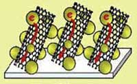 The photocatalytic activity of nanostructured semiconductor films has been widely explored in designing solar cells, solar hydrogen production, and environmental remediation. Of particular interest is the dye-sensitized solar cell (DSSC) which uses nanostructured titanium dioxide films modified with sensitizing dyes. Despite the initial success of achieving 10% solar conversion efficiency, the effort to further improve their performance has not been very successful. A major hurdle in attaining higher photoconversion efficiency in such nanostructured electrodes is the transport of electrons across the particle network. The photogenerated electrons in nanostructured films for example have to travel through the network of semiconductor particles and encounter many grain boundaries during the transit. Such a random transit path for the photogenerated electrons increases the probability of their recombination with oxidized sensitizer. With the recent advance in the design of nanotube and nanowire architecture, it should be possible to use such one-dimensional nanostructures to direct the flow of photogenerated charge carriers. The obvious challenge is to use nanowire or nanotube networks as support to anchor light-harvesting semiconductor particles and facilitate the electron transport to the collecting electrode surface in a solar cell. Researchers now have demonstrated that single wall carbon nanotube (SWCNT) architecture when employed as conducting scaffolds in a titanium dioxide semiconductor based photoelectrochemical cell can boost the photoconversion efficiency by a factor of 2.
Feb 28th, 2007
 With an increased focus on alternative sources of cheap, abundant, clean energy, solar cells are receiving lots of attention. Harnessing the power of the sun to replace the use of fossil fuels holds tremendous promise. One way to do this is through the use of solar, or photovoltaic, cells. Until now, solar cells that convert sunlight to electric power have been dominated by solid state junction devices, often made of silicon wafers. Thanks to nanotechnology, this is now being challenged by the development of a new generation of solar cells based on thin film materials, nanocrystalline materials and conducting polymeric films. These offer the prospects of cheaper materials, higher efficiency and flexible features. This has opened up new opportunities in solar cell research and development and, consequently, there is considerable investor interest in solar nanotechnology startups. Both inventors and investors are betting that flexible sheets of solar cells used to harness the sun's strength will ultimately provide a cheap and efficient source of energy.
Feb 22nd, 2007
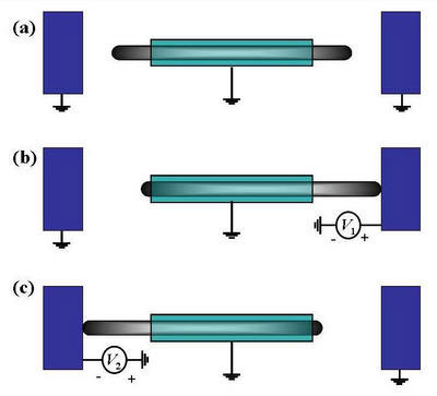 Non-volatile random access memory (NVRAM) is the general name used to describe any type of random access memory which does not lose its information when power is turned off. This is in contrast to the most common forms of random access memory today, DRAM and SRAM, which both require continual power in order to maintain their data. NVRAM is a subgroup of the more general class of non-volatile memory types, the difference being that NVRAM devices offer random access, as opposed to sequential access like hard disks. The best-known form of NVRAM memory today is flash memory, which is found in a wide variety of consumer electronics, including memory cards, digital music players, digital cameras and cell phones. One problem with flash memory is its relatively low speed. Also, as chip designers and engineers reach size barriers in downscaling the size of such chips, the research focus shifts towards new types of nanomemory. Molecular-scale memory promises to be low-power and high frequency: imagine a computer that boots up immediately on powering up and that writes data directly onto its hard drive making saving a thing of the past. Researchers are designing the building blocks for this type of memory device using telescoping carbon nanotubes as high-speed, low power microswitches. The design would allow the use of these binary or three-stage switches to become part of molecular-scale computers.
Feb 14th, 2007
 For several years now, researchers have documented the many intriguing mechanical and electrical properties of carbon nanotubes (CNTs). Some researchers have focused on the optical properties of CNTs. Studying the passive optical response of CNTs they have revealed the manner in which CNTs' optical properties are related to shape and structure of CNTs. It was found that periodic CNT arrays exhibit Bragg diffraction, photonic bandgap properties, and plasmonic resonance; nonperiodic CNT arrays interact with light waves similarly to the way in which radio antennae interact with radio waves. In conventional radio antenna theory an antenna acts as a resonator of the external electromagnetic radiation. Scientists now have demonstrated that a single multiwall carbon nanotube (MWCNT) acts as an optical antenna, whose response is fully consistent with conventional radio antenna theory.
Feb 13th, 2007
 Carbon nanotubes (CNTs) belong to the most exciting nanomaterials discovered so far and the buzz associated with them has to do with their amazing properties. Depending on their structure, they can be metals or semiconductors. They exhibit extraordinary mechanical properties, which make them extremely strong materials with good thermal conductivity. Their tensile strength is several times that of steel. These characteristics have generated strong interest in their possible use in reinforced composites, nanoelectronics, nanomechanical devices, circuits and computers. Single-wall nanotubes (SWNTs) are an intriguing variant of carbon nanotubes because they exhibit important electrical properties that are not shared by the multi-walled carbon nanotubes (MWNT). SWNTs are the most likely candidate for miniaturizing electronics toward the nanoscale. Because of their enormous commercial potential, universities, start-ups, and corporations have aggressively sought patent protection on nanotube-based products. A recent legal paper identifies key patents claiming compositions of matter, methods of production, and products incorporating nanotubes. The authors summarize potential patent invalidity arguments that may be raised against certain patents in the field and explain how the patent landscape impacts the commercialization of nanotube-based products. A proposed "Nanotube Patent Forum" could be a means for industry to facilitate cost-effective licensing transactions between patent holders and manufacturers.
Jan 31st, 2007
The discovery of numerous nanomaterials has added a new dimension to the rapid development of nanotechnology. Consequently, the professional and public exposure to nanomaterials is supposed to increase dramatically in the coming years. Especially, carbon-based nanomaterials (CBNs) are currently considered to be one of the key elements in nanotechnology. Their potential applications range from biomedicine through nanoelectronics to mechanical engineering. Thus, it is primordial to know the health hazards related to their exposure. As the public calls for safety studies get louder more and more researchers begin to study the potential toxicity of nanomaterials. Especially carbon-based nanomaterials, due to their numerous and wide-ranging applications and increasing real life usage, get nanotoxicological attention. Scientists in Switzerland studied the toxicity of carbon- based nanomaterials (nanotubes, nanofibers and nanowires) as a function of their aspect ratio and surface chemistry. Their work clearly indicates that these materials are toxic while the hazardous effect is size-dependent.
Jan 19th, 2007
With its historic development tracing back to the Bronze Age, welding serves modern industry in broad areas such as construction, manufacturing, and engineering. Spot welding,a type of resistance welding used to weld various sheet metals, was originally developed in the early 1900s. The process uses two shaped copper alloy electrodes to concentrate welding current and force between the materials to be welded. The result is a small "spot" that is quickly heated to the melting point, forming a nugget of welded metal after the current is removed. Perhaps the most common application of spot welding is in the automobile industry, where it is used almost universally to weld the sheet metal forming a car. Spot welders can also be completely automated, and many of the industrial robots found on assembly lines are spot welders. With the continuing development of bottom-up nanotechnology fabrication processes, with self-assembly at its core, spot welding may likewise play an important role in interconnecting carbon nanotubes (CNTs), nanowires, nanobelts, nanohelixes, and other nanomaterials and structures for the assembly of nanoelectronics and nanoelectromechanical systems (NEMS).
Jan 2nd, 2007
 Subscribe to our Nanotechnology Spotlight feed