| Posted: Sep 09, 2014 | |
Flexible high-performance FinFETs with a bending radius of 0.5 mm |
|
| (Nanowerk Spotlight) The emergence of the Internet of Everything demands additional improvements in today's – mostly rigid – electronics: They have to be flexible, stretchable, reconfigurable. Whereas state-of-the-art electronic components have extraordinary benefits from performance, energy efficiency, ultra large scale integration density and cost perspectives, flexible electronics hasn't reached these performance levels yet. | |
| The semiconductor industry's most advanced device architecture are FinFETs (or 3D tri-gate transistors). These are 3D field effect transistors that rise above the planar substrate where the channels are vertically aligned on the planar area in arrays of ultra-thin silicon fins bordered by multiple gates. FinFETs show a nearly 40% performance improvement and 50% reduced power consumption over any other state-of-the-art transistors. | |
| The flexibility required when fabricating flexible electronic components has led to the use of plastic substrates and different transfer techniques to fabricate flexible devices. However, one of the biggest obstacles to mass adoption of flexible electronics has been the incompatibility with industry's state-of-the-art silicon-based CMOS processes – which still produce about 90% of today's electronics. | |
| Researchers have now developed a new process that can be used to reduce the thickness of the silicon substrate until the required flexibility is obtained. Reporting their findings in the September 3, 2014 online edition of ACS Nano ("Flexible Nanoscale High-Performance FinFETs"), they demonstrate a flexible (0.5 mm bending radius) nanoscale FinFET on silicon-on-insulator using a back-etch based substrate thinning process. | |
 |
|
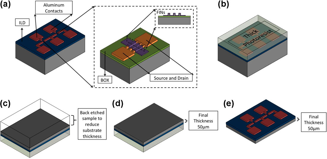
| Fabrication process flow: (a) fabricated FinFET devices on standard 90 nm SOI with 150 nm BOX; (b) PR coating for chip-protection during back etch process; (c) FinFET die etched back using back grinding technique; (d) FinFET devices on flexible silicon substrate (50 µm thick); and (e) PR removal and final device testing. (Reprinted with permission by American Chemical Society) (click on image to enlarge) | |
| These FinFETs show an unprecedented bending radius of just 0.5 mm. Importantly, compared to conventional FinFETs on rigid-bulk-traditional silicon-on-insulator (SOI) substrate, they show no performance degradation. | |
| "I'd like to point out that our process is in every regard industry compatible and there is no need of using abrasive processes," Muhammad Mustafa Hussain, an Associate Professor of Electrical Engineering at King Abdullah University of Science and Technology (KAUST), tells Nanowerk. | |
| For the last 2 years, Hussain and his team have been working in the area of flexible electronics in order to find a way of transforming commonly used rigid electronic devices into flexible ones using existing industry-standard processes. | |
| In previous Nanowerk Spotlights we have reported on these efforts to develop different method to transform conventional electronics into flexible ones without compromising cost, yield, performance and efficiency (see for instance: "Flexible silicon-on-polymer sub-20 nm FinFETs without performance loss"). | |
| In this new work, the researchers used a soft back-etch process to thin down the SOI wafer with FinFETs on it while protecting the devices with a photoresist coating. | |
| Semiconductor wafers are routinely thinned in order to minimize the thickness of the assembled package. This is done with a process called backgrinding where the wafer substrate is ground from the backside and thinned down to 50-75 µm. | |
| Although widely used, two issues limit its usage for ultra-thin flexible and stretchable wearable electronics: the process is abrasive and could damage the devices on the other side of the substrate; since the process can grind down to only 50 µm it can provide some flexibility but not a lot. | |
| "Compared to that technique our novel process gently back-etches down to less than 50 µm, ultimately resulting in very high flexibility including a demonstrated 0.5 mm bending radius which is unprecedented in the context of bending a solid state material like silicon," notes Hussain. "Compared to backgrinding, our process not only allows for a greater thinning range but it also is much gentler in order to protect nanoscale devices on the front side of the substrate," says Hussain. "In essence, our present technique is a novel way of replacing backgrinding during the fabrication of electronic components." | |
| Now that the team has demonstrated 3D transistors on a flexible, inorganic platform using only industry compatible processes, they expect that in the near future they will be able to show circuit-scale devices using the same technique. | |
| "Although there are many challenges that need to be overcome before we can obtain a complete flexible circuit, these issues are solvable and hence we expect that with careful design, we will be able to demonstrate the first flexible very large scale circuitry using only silicon compatible processes and without the need of abrasive or destructive techniques such as backgrinding," Hussain concludes. | |
 By
Michael
Berger
– Michael is author of three books by the Royal Society of Chemistry:
Nano-Society: Pushing the Boundaries of Technology,
Nanotechnology: The Future is Tiny, and
Nanoengineering: The Skills and Tools Making Technology Invisible
Copyright ©
Nanowerk LLC
By
Michael
Berger
– Michael is author of three books by the Royal Society of Chemistry:
Nano-Society: Pushing the Boundaries of Technology,
Nanotechnology: The Future is Tiny, and
Nanoengineering: The Skills and Tools Making Technology Invisible
Copyright ©
Nanowerk LLC
|
|
|
Become a Spotlight guest author! Join our large and growing group of guest contributors. Have you just published a scientific paper or have other exciting developments to share with the nanotechnology community? Here is how to publish on nanowerk.com. |
|