Nanotechnology News – Latest Headlines
Video camera that records at the speed of thought
European researchers who created an ultra-fast, extremely high-resolution video camera have enabled dozens of medical applications, including one scenario that can record 'thought' processes travelling along neurons.
October 13, 2009 Read more
UAlbany programs will highlight growing impact of nanotechnology
The University at Albany today announced an extensive schedule of events and activities to be held during its month-long celebration of NANOvember.
October 13, 2009 Read more
Highspeed-Datennetze mit Nanoantennen
KIT-Wissenschaftlern ist es nun erstmals gelungen, kleinste optische Nanoantennen aus Gold gezielt und reproduzierbar anzufertigen.
October 13, 2009 Read more
Current safety equipment may not be adequate for nanoprotection
Canadian engineers suggest that research is needed into the risks associated with the growing field of nanotechnology manufacture so that appropriate protective equipment can be developed urgently.
October 13, 2009 Read more
SOI Industry Consortium announces SOI design clinic at ARM TechCon3
The SOI Industry Consortium today announced an initiative to deliver a silicon on insulator (SOI) educational event in conjunction with ARM TechCon3 to help the electronics industry reap the benefits of SOI.
October 13, 2009 Read more
Novel plasmonic nanorod metamaterial for sensor applications
Researchers at Oregon State University and other institutions have developed a new plasmonic nanorod metamaterial using extraordinarily tiny rods of gold that will have important applications in medical, biological and chemical sensors.
October 13, 2009 Read more
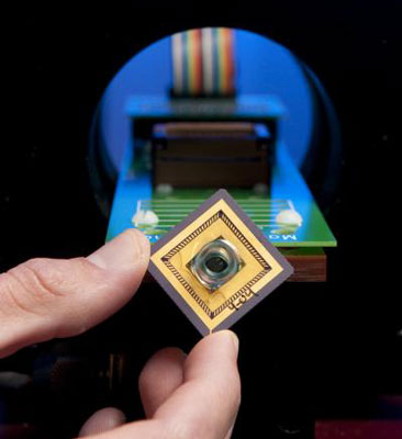
Magnetic nanosensors dramatically improve cancer detection
Improved magneto-nano sensor chips are up to 1,000 times more sensitive than current methods of cancer detection - can scan any bodily fluid with high accuracy and search for up to 64 different cancer-associated proteins simultaneously.
October 13, 2009 Read more
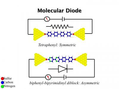
Nanoelectronics researchers make single-molecule diode
Recently, at Arizona State University's Biodesign Institute, N.J. Tao and collaborators have found a way to make a key electrical component on a phenomenally tiny scale.
October 13, 2009 Read more
Neues Verfahren zur Graphen-Gewinnung
Eine Arbeitsgruppe aus Chemikern und Physikern der Universitaet des Saarlandes hat ein grundlegend neues Verfahren entwickelt, mit dem graphenbeschichtete Oberflaechen hergestellt werden koennen.
October 13, 2009 Read more
European Environment Bureau assesses critical nanotechnology governance issues
The European Environmental Bureau (EEB), Europe's largest federation of environmental citizens' organizations, launched a report outlining the critical governance structures needed for the safe development and use of nanotechnologies.
October 13, 2009 Read more
Max Planck Innovation grants rights for developing new nanoscopic method to Leica Microsystems
Max Planck Innovation, the technology transfer organization of the Max Planck Society, grants Leica Microsystems, Wetzlar, an exclusive license for implementing the latest generation of optical microscopes with a resolution far below the diffraction limit (nanoscopes).
October 13, 2009 Read more
UC Santa Barbara and IME of Singapore agree 'green electronics' research collaboration
UC Santa Barbara and the Institute of Microelectronics (IME) of Singapore have entered into a 'green electronics' research collaboration agreement focused on developing ultra-efficient nanoscale transistors and exploring their circuit-level functionality.
October 12, 2009 Read more
Max-Planck-Innovation lizenziert Nanoskopieverfahren an Leica Microsystems
Leica Microsystems, Wetzlar, erhaelt von Max-Planck-Innovation, der Technologietransfer-Organisation der Max-Planck-Gesellschaft, die Exklusivlizenz fuer die Umsetzung der neuesten Generation optischer Mikroskope mit Aufloesung weit unterhalb der Beugungsgrenze (Nanoskope).
October 12, 2009 Read more
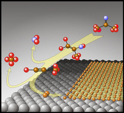
Engineers control the electronic properties of graphene by functionalizing it with gold
In an effort to make graphene more useful in electronics applications, Kansas State University engineers made a golden discovery - gold 'snowflakes' on graphene.
October 12, 2009 Read more
University of Washington breaks ground on nations' largest molecular engineering building
The completed building will consist of a 28,000-square-foot basement, an 8,000-square-foot sub-basement, and four above-ground levels each measuring about 12,000 square feet. The total building is about 90,000 square feet including hallways, utilities and common spaces.
October 12, 2009 Read more
Cockroft Institute Awarded 16 million pounds to boost accelerator research
The Cockcroft Institute, a partnership between the Universities of Liverpool, Lancaster and Manchester, has been awarded 16.4million pounds to further research into accelerator science and technology.
October 12, 2009 Read more
 Subscribe to our Nanotechnology News feed