Domain Wall: Structure, Dynamics, and Nanotechnology Applications
What is a Domain Wall?
A domain wall is the thin interfacial region inside a ferroic material where an order parameter – magnetization, electric polarization, or spontaneous strain – changes from one domain orientation or variant to another.
Ordered materials such as ferromagnets, ferroelectrics, and ferroelastics often lower their total energy by splitting into uniformly ordered regions called domains. Where two domains meet, the order parameter cannot usually switch abruptly without paying a large exchange, electrostatic, elastic, or gradient-energy cost. Instead, it changes across a finite transition region: the domain wall. In a ferromagnet, the magnetization may rotate from one easy direction to another; in a ferroelectric, the electric polarization reverses or changes between crystallographically allowed orientations; in a ferroelastic crystal, the spontaneous strain switches between twin variants.
A domain wall is not the same thing as a grain boundary. A grain boundary separates two crystals with different lattice orientations, while a domain wall can exist inside a single continuous crystal whose lattice remains largely coherent across the wall. What changes is the magnetic, electric, or strain state, not necessarily the crystallographic grain.
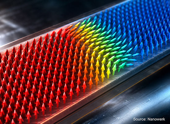
Domain walls form because a uniformly ordered sample may produce large stray-field, electrostatic, or elastic energies. Splitting the material into domains reduces those long-range energies, but every wall costs local energy. The observed domain pattern is the compromise between these competing terms. Magnetic domain walls can range from a few nanometres to about 100 nm wide, depending on the material and geometry. In many neutral ferroelectric perovskite walls, the structural polarization change is only one to two unit cells wide, although charged domain walls and electronically screened regions can be wider. These natural length scales matter directly in nanowires, thin films, and nanocrystalline materials.
Key takeaways:
- A domain wall is the nanoscale transition region between two domains of uniform order in a ferroic material.
- Its width is set by the competition between a smoothing energy, such as exchange or gradient energy, and an energy that favours preferred orientations, such as magnetic or ferroelectric anisotropy.
- Magnetic domain walls are usually nanometres to tens of nanometres wide; many neutral ferroelectric walls are only a few angstroms wide at the structural level.
- Domain walls can be moved with magnetic fields, electric fields, stress, or spin-polarized currents, and some walls host electronic properties not found in the surrounding material.
How a Domain Wall Forms: Energy Balance and Wall Types
The width and internal structure of a domain wall are set by competing energy terms. In a ferromagnet, exchange interaction prefers neighbouring spins to remain parallel and therefore favours a slow, wide rotation. Magnetic anisotropy favours alignment along specific crystallographic directions and therefore favours a sharper wall. The equilibrium wall width scales approximately as the square root of the ratio between exchange stiffness and anisotropy energy density. Materials with strong anisotropy, such as many rare-earth permanent magnets, have narrow walls; soft magnetic alloys with weak anisotropy can have much wider walls.
The same logic applies in ferroelectrics and ferroelastics, although the microscopic terms differ. Ferroelectric gradient energy resists abrupt polarization changes, while electrostatic energy, elastic compatibility, and crystal anisotropy determine which wall orientations are stable. Neutral 180° ferroelectric walls can be atomically sharp, whereas charged walls require screening by carriers, defects, or ionic motion and may have a broader electronic or chemical profile than their crystallographic core.
In magnetic materials, the two classic wall textures are Bloch and Néel walls. In a Bloch wall, the magnetization rotates within the plane of the wall, which helps avoid magnetic charge on the wall surfaces in bulk magnets and thicker films. In a Néel wall, the magnetization rotates in the plane normal to the wall. Néel walls are often favoured in very thin films and nanostructures, where the sample shape and interfaces make the Bloch configuration less favourable. In ultrathin metallic multilayers grown on heavy-metal underlayers such as platinum or tungsten, broken inversion symmetry at the interface can produce the Dzyaloshinskii–Moriya interaction (DMI), an antisymmetric exchange interaction that favours a particular sense of spin rotation. The result is a chiral Néel wall with fixed handedness. This fixed chirality is one ingredient that allows spin-orbit torques to drive walls deterministically along a racetrack, an important requirement for spintronics devices.
Ferroelectric domain walls can also be classified by how the polarization changes across them. Some are nearly Ising-like, with the polarization magnitude passing through a small value while its direction reverses. Others have Bloch-like or Néel-like components, meaning the polarization rotates partly within or normal to the wall plane. When the wall orientation creates a head-to-head or tail-to-tail arrangement of polarization, bound charge accumulates at the wall. Such charged domain walls must be screened by free carriers, defects, or ions, and they often become electrically conductive even when the surrounding crystal is insulating.
Why Domain Walls Matter at the Nanoscale
When a magnet or ferroelectric is patterned to dimensions comparable to its natural domain size, the wall is no longer a small internal detail. A nanoparticle below the single-domain limit, typically tens of nanometres for many ferromagnets, contains no domain wall and behaves as one giant magnetic moment. Slightly larger particles and patterned magnetic nanoparticles may host one or a few trapped walls whose pinning, mobility, and switching fields control the entire device response. Similar size effects influence hard-disk media, magnetic sensors based on giant magnetoresistance, and storage elements based on magnetic tunnel junctions.
A second nanoscale consequence is that the wall itself can occupy a substantial fraction of the device. In a 100 nm wide magnetic nanowire, a 20–30 nm Néel wall is not a negligible boundary; it is a functional object whose spin texture, chirality, edge pinning, and interaction with engineered notches determine how the device works. Whole subfields of nanomagnetism and ferroelectric nanoelectronics are devoted to creating, moving, pinning, and reading out domain walls at precise positions.
Comparing Magnetic, Ferroelectric, and Ferroelastic Domain Walls
Domain walls in different ferroic systems share the same basic origin, but their thicknesses, mobilities, and functional properties differ substantially. The values below are typical orders of magnitude and depend strongly on material composition, film thickness, strain state, temperature, and device geometry.
| Wall type | Typical thickness | Order parameter | Driving stimuli | Characteristic functions |
|---|---|---|---|---|
| Bloch wall (bulk or thicker ferromagnet) | ~ 30–100 nm | Magnetization rotating within the wall plane | Magnetic field, spin-transfer torque | Soft-magnetic domain structures, magnetic-force microscopy contrast |
| Néel wall (thin film or nanostructure) | ~ 5–30 nm | Magnetization rotating in the plane normal to the wall | Field, current, spin-orbit torque | Racetrack-memory concepts, domain-wall logic, patterned nanomagnets |
| Chiral Néel wall (heavy-metal/ferromagnet interface) | ~ 5–20 nm | Magnetization with fixed handedness set by DMI | Spin Hall current, spin-orbit torque | High-velocity racetracks, deterministic wall motion, skyrmion nucleation |
| Neutral ferroelectric 180° wall | ~ 0.3–1 nm structural core in many perovskites | Electric polarization reversal, usually uncharged when wall orientation avoids bound charge | Electric field, strain, tip bias | Ferroelectric memory, piezoelectric response, nanoscale domain engineering |
| Charged ferroelectric wall | ~ 1–5 nm screened electronic or chemical region, often material-dependent | Polarization in head-to-head or tail-to-tail configuration | Electric field, charge injection, ionic defect redistribution | Conductive two-dimensional channels, memristive devices, reconfigurable nanoelectronics |
| Ferroelastic / twin wall | ~ 1–10 nm | Spontaneous strain or crystallographic variant | Mechanical stress, electric field in coupled materials | Shape-memory effects, domain engineering, multiferroic coupling |
These contrasts explain why magnetic and ferroelectric domain-wall devices are designed differently. Magnetic walls are comparatively wide and can be driven rapidly by currents through spin-transfer and spin-orbit torques. Ferroelectric walls are much thinner at the structural level and are controlled primarily by voltage, but their bound-charge environment and defect chemistry can make them excellent reconfigurable electronic channels.
Manipulating Domain Walls
Magnetic domain walls can be moved by an applied magnetic field. At low fields, the wall velocity generally rises with field. Above a dynamic threshold known as Walker breakdown, the internal wall structure begins to precess or oscillate, which can reduce the average velocity. Current-driven motion added a second route: a spin-polarized current passing through a ferromagnetic nanowire transfers spin angular momentum to the wall and can push it along the wire. The 2008 racetrack-memory proposal by Stuart Parkin and colleagues at IBM showed how this mechanism could, in principle, replace mechanical motion in disk drives with all-electronic shifting of magnetic bits along nanowires.
Spin-orbit torques produced by the spin Hall effect in a heavy-metal underlayer are often more efficient than conventional spin-transfer torque in ultrathin multilayers. Combined with interfacial DMI that stabilizes chiral Néel walls, spin-orbit torques can drive uniform domain-wall motion at hundreds of metres per second, with reports approaching or exceeding one kilometre per second in optimized synthetic antiferromagnetic or ferrimagnetic stacks. Pinning at edge roughness, grain boundaries, defects, and engineered notches remains a central practical constraint because it determines the current density needed for reliable motion. Recent domain-wall logic demonstrations show that the same physical toolkit can implement electrically controlled inverters and cascaded logic gates, although these concepts remain research-stage technologies.
Ferroelectric domain walls move under applied electric fields and, in some materials, under stress, charge injection, or chemical gradients. Unlike most defects in solids, they can often be created, displaced, and erased reversibly within a single device. Conductive atomic-force-microscope tips and piezoresponse force microscopy are widely used to write domain patterns, move walls, and read local wall conduction. This controllability is the basis for ferroelectric domain-wall nanoelectronics and for device concepts in which resistance changes because the number, position, or charge state of the walls changes.
Applications of Domain Walls
Racetrack memory and domain-wall logic
In racetrack memory, data are encoded as a train of magnetic domains separated by domain walls along a narrow magnetic wire. Current pulses shift the domain train past fixed read and write elements, so the data move electronically while the read head remains stationary. Because the storage wires can, in principle, be arranged vertically on a silicon chip, racetrack memory was proposed as a route to dense, non-volatile storage with solid-state operation and no moving mechanical parts. It remains a research technology rather than a mainstream commercial memory, mainly because reliable wall motion, low operating current, and large-scale integration are difficult to achieve simultaneously.
Closely related domain-wall logic schemes use the position or chirality of a wall in a nanowire network to represent a bit. Logic operations can be performed by allowing walls to interact, branch, annihilate, or move through engineered junctions. Chiral coupling and spin-orbit torque have made these schemes more robust, but practical circuits still face the same problems as racetrack memory: pinning, variability, thermal fluctuations, and the need for reliable readout at CMOS-compatible energy and voltage levels.
Ferroelectric memristors and neuromorphic devices
In ferroelectric thin films and crystals, domain walls can act as movable electronic elements. A landmark 2009 demonstration by Seidel and colleagues showed room-temperature electronic conduction at ferroelectric domain walls in otherwise insulating bismuth ferrite. Subsequent work in lithium niobate, hexagonal manganites, barium titanate, PZT, and related materials showed that wall conductivity can be tuned by wall charge, strain, oxygen vacancies, local band bending, and electrochemical screening.
This tunability makes ferroelectric walls attractive for memristors and neuromorphic synapses. A device can store an analogue resistance state if voltage pulses create more walls, remove walls, move conductive walls into or out of a current path, or change the screening charge around a charged wall. In multiferroics, domain walls can also couple ferroelectric polarization to magnetic order, raising the possibility of magnetoelectric memories switched by electric fields rather than large currents.
Imaging and Characterization
Magnetic domain walls are imaged by several complementary methods. Magnetic force microscopy detects stray magnetic fields above walls. Lorentz transmission electron microscopy maps in-plane magnetization through electron-beam deflection and can resolve nanoscale domain structures. Magneto-optical Kerr microscopy follows larger domains dynamically, while element-specific synchrotron X-ray techniques can resolve buried magnetic layers and track wall motion on very short timescales.
For ferroelectric walls, piezoresponse force microscopy is the standard tool for mapping polarization through the local converse piezoelectric response. Conductive atomic force microscopy maps current at charged or otherwise conductive walls. High-resolution transmission electron microscopy and scanning transmission electron microscopy can resolve unit-cell-scale polarization shifts, octahedral distortions, and strain fields across a wall. Combining these structural, electrical, and chemical probes is often essential because the conductivity of a ferroelectric wall may depend as much on defects and screening charges as on the ideal wall geometry.
Challenges and Future Perspectives
Despite intense research since the racetrack-memory proposal, domain-wall memory and logic have not yet displaced established CMOS technologies. The major barriers are stochastic pinning at defects and edges, device-to-device variability, thermal stability of closely spaced walls, reliable nucleation and deletion of walls, and the still-substantial current densities needed for fast motion. Synthetic antiferromagnets, ferrimagnets, and antiferromagnetic domain walls are active research directions because they can reduce stray fields and may support faster dynamics than conventional ferromagnetic walls.
For ferroelectric walls, the principal challenges are reproducible wall conduction, endurance under repeated switching, retention of written wall states, and compatibility with silicon processing. Conductive walls can be extremely sensitive to local defects, stoichiometry, humidity, electrode chemistry, and screening conditions. That sensitivity is a problem for manufacturing but also a source of functionality: it allows domain walls to behave as reconfigurable, nanoscale electronic channels whose resistance, position, and connectivity can be programmed.
The broader trend is that domain walls are no longer treated only as passive boundaries between useful domains. They are increasingly studied as functional two-dimensional objects with their own electronic structure, transport behaviour, chirality, dynamics, and coupling to other nanoscale textures such as skyrmions. As device dimensions approach the intrinsic length scales of ferroic order, domain walls are likely to remain important as movable, writable, and reconfigurable elements in solid-state information processing.
FAQ: Domain Wall
What is a domain wall in simple terms?
A domain wall is the thin transition region inside an ordered material such as a magnet, ferroelectric, or ferroelastic where the material changes from one domain orientation to another. The domains on either side are uniformly ordered; the wall is the boundary region where the magnetic, electric, or strain state changes. In many magnetic materials a domain wall is a few nanometres to about 100 nm wide, while many neutral ferroelectric walls are only one or two unit cells wide at the structural level.
What is the difference between a Bloch wall and a Néel wall?
Both are types of magnetic domain walls and differ in the plane in which the magnetization rotates. In a Bloch wall, the magnetization rotates within the wall plane. In a Néel wall, it rotates in the plane normal to the wall. Bloch walls are common in bulk magnets and thicker films, while Néel walls are favoured in many thin films and nanostructures. In ultrathin heavy-metal/ferromagnet stacks, interfacial Dzyaloshinskii–Moriya interaction can fix the handedness of a Néel wall and make it chiral.
How fast can a magnetic domain wall move?
In standard ferromagnetic nanowires, current-driven domain-wall velocities are often in the range of tens to a few hundred metres per second. In optimized chiral, ferrimagnetic, or synthetic-antiferromagnetic stacks, velocities approaching or exceeding one kilometre per second have been reported. The practical speed depends on pinning, heating, current density, wall structure, and whether dynamic instabilities such as Walker breakdown occur.
What is racetrack memory and why does it use domain walls?
Racetrack memory is a non-volatile storage concept in which data bits are represented by magnetic domains separated by domain walls along a narrow wire. Current pulses shift the domain train past fixed read and write elements, so the information moves electronically through the wire. The concept was proposed as a route to dense, solid-state storage, especially if vertical nanowires could be integrated on chips, but it remains a research technology rather than a mainstream commercial memory.
Are ferroelectric domain walls electrically conductive?
Some ferroelectric domain walls are more conductive than the surrounding crystal, even when the bulk material is insulating. Conductivity can arise from bound-charge screening, local band bending, strain, defects such as oxygen vacancies, or changes in the wall's electronic structure. A landmark 2009 study showed room-temperature conduction at domain walls in bismuth ferrite, and later work extended conductive-wall concepts to charged walls and other ferroelectric materials.
What is a charged domain wall?
A charged domain wall is a ferroelectric wall in which the polarization vectors on the two sides create bound charge at the wall, commonly in head-to-head or tail-to-tail arrangements. That charge must be screened by mobile electrons, holes, ionic vacancies, or other defects. The screening region can make the wall electronically conductive, chemically active, and useful as a reconfigurable nanoscale channel.
Related Concepts
Nanomagnetism | Magnetic tunnel junctions | Giant magnetoresistance | Skyrmions | Multiferroics | Memristors
Further Reading
Nature Materials, Conduction at domain walls in oxide multiferroics
Reviews of Modern Physics, Domain wall nanoelectronics
Nature Reviews Materials, Ferroelectric domain walls for nanotechnology
Journal of Physics D: Applied Physics, Magnetic domain walls: types, processes and applications
