Charged Domain Walls: Reconfigurable Conductive Interfaces in Ferroelectric Materials
What are Charged Domain Walls?
Charged domain walls (CDWs) are ultrathin interfaces – typically only a few nanometers wide – that separate regions of different polarization orientation within a ferroelectric material and carry a net bound electrical charge. Unlike conventional neutral domain walls, where the normal component of spontaneous polarization remains continuous across the boundary, CDWs arise when the polarization vectors of adjacent domains point toward or away from the wall, creating a local discontinuity. This bound charge must be compensated by free carriers – electrons, holes, or mobile ions – and the resulting accumulation of screening charges can produce metallic-like conductivity in an otherwise insulating material.
Principle Behind Charged Domain Walls
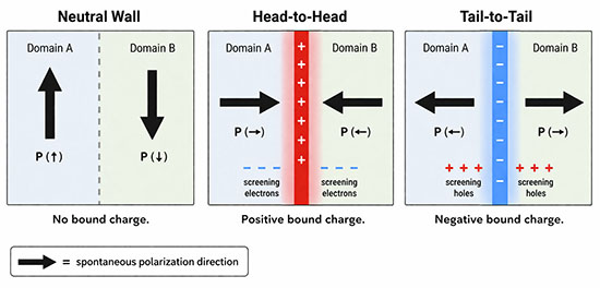
In ferroelectric materials, spontaneous polarization divides the crystal into domains whose polarization directions are determined by the material's symmetry. The boundaries between these domains are called domain walls. When the polarization vectors on either side of a wall have a normal component that changes sign across the boundary, a bound charge density appears at the interface. This situation arises in two configurations: head-to-head walls, where polarization vectors point toward each other (producing positive bound charge), and tail-to-tail walls, where they point away from each other (producing negative bound charge).
The electric field generated by this bound charge is energetically costly and, if left uncompensated, can destabilize the ferroelectric state in the adjacent domains. Stability therefore requires charge screening by mobile carriers. In semiconducting ferroelectrics, band bending near the wall drives the accumulation of electrons or holes, forming a quasi-two-dimensional electron or hole gas at the wall.
The screening charge concentration at a strongly charged wall can reach approximately 1020 cm-3, an extremely high value for nominally insulating wide-bandgap materials. This mechanism transforms the domain wall into a conductive sheet that can be created, moved, and erased by an applied electric field.
Types of Charged Domain Walls
Charged domain walls can be classified according to the magnitude of their bound charge and the angle between the polarization and the wall plane. The two principal categories are strongly charged and weakly charged walls, each with distinct stability requirements and screening behavior.
Strongly Charged Domain Walls
Strongly charged domain walls (SCDWs) occur when the bound charge is large enough that, in the absence of screening, the resulting depolarization field would destroy ferroelectricity in the adjacent domains. These walls require nearly complete charge compensation to remain stable. In proper ferroelectrics such as BaTiO3, SCDWs can host a free-electron gas with conductivities many orders of magnitude higher than the surrounding bulk. The wall–domain conductivity contrast has been measured at up to 13 orders of magnitude in some materials.
Weakly Charged Domain Walls
Weakly charged domain walls (WCDWs) carry a smaller bound charge, arising when the wall deviates slightly from its electrostatically neutral orientation. The depolarization field is insufficient to destabilize the ferroelectric order, so WCDWs can exist even without significant screening. These walls form transiently during every 180° polarization switching event because the expanding domain nucleus inevitably produces wall segments inclined to the polarization axis. Although their conductivity enhancement is modest compared to SCDWs, WCDWs are far more common and play a role in switching dynamics.
Head-to-Head and Tail-to-Tail Configurations
Head-to-head walls accumulate positive bound charge and attract electrons for compensation, whereas tail-to-tail walls accumulate negative bound charge and attract holes or positively charged ionic species. This asymmetry means that head-to-head and tail-to-tail walls in the same material can exhibit fundamentally different electronic transport characteristics, effectively creating nanoscale p–n junctions or electronic inversion layers at the wall.
Significance in Nanotechnology
Charged domain walls represent a unique class of functional interface at the nanoscale. Unlike conventional heterojunctions, thin film interfaces, or grain boundaries, CDWs are compositionally homogeneous – they exist within a single material. This means they can be written, erased, and repositioned inside a functioning device using only an applied electric field, offering a degree of spatial reconfigurability that fixed interfaces cannot match.
The effective thickness of a CDW is typically on the order of 1–10 nm, approaching the unit-cell level in some systems. This extreme spatial confinement, combined with the high carrier concentrations produced by charge screening, gives rise to properties reminiscent of quantum effects observed in other low-dimensional systems. The walls can be viewed as reconfigurable two-dimensional conducting sheets embedded in an insulating matrix – a combination of mobility and conductivity that is difficult to achieve with any other material architecture.
Key Properties of Charged Domain Walls
Electronic Conductivity
The most striking property of CDWs is their dramatically enhanced electrical conductivity relative to the host material. In materials such as BaTiO3 and the hexagonal rare-earth manganites (for example ErMnO3), the quasi-two-dimensional carrier gas at a strongly charged wall produces conductivity comparable to that of a metal within a material that is otherwise a wide-bandgap insulator. This conductivity can be switched on and off reversibly by transforming the wall between charged and neutral configurations using an applied electric field. Scanning probe techniques such as conductive atomic force microscopy (C-AFM) and piezoresponse force microscopy (PFM) are widely used to map and manipulate these conductive walls at the nanoscale.
Rectification and Nonlinear Transport
Because head-to-head and tail-to-tail walls host carriers of opposite polarity, individual domain walls can exhibit asymmetric current–voltage characteristics similar to those of a semiconductor diode. Electrical half-wave rectification has been demonstrated at ferroelectric domain walls, and the electrode–wall junction displays pronounced nonlinear responses under alternating current. These effects enable domain walls to emulate the behavior of conventional electronic components at dimensions far below those achievable with lithographic fabrication.
Electromechanical Response
CDWs can enhance the electromechanical response of a ferroelectric material. The presence of charged walls and their associated screening charges modifies the local polarization landscape and susceptibility, which can increase the effective piezoelectric coefficients. In addition, the steep strain gradients that exist at domain walls give rise to flexoelectric contributions that further couple mechanical deformation to polarization. This enhancement grows with increasing CDW density, suggesting that engineered arrays of charged walls could improve the performance of nanoactuators and electromechanical sensors.
Photoconductivity
Light illumination can modify the charge state and conductivity of domain walls, an effect that links CDW physics to the broader field of nanophotonics. Photogenerated carriers alter the screening balance at the wall, enabling optical control of domain-wall conductivity. This photoconductivity opens pathways for light-driven reconfiguration of conductive channels within a ferroelectric device.
Materials Hosting Charged Domain Walls
Perovskite Ferroelectrics
Classic perovskite ferroelectrics such as BaTiO3, PbTiO3, and (Pb,Sr)TiO3 thin films are among the most studied hosts for CDWs. In BaTiO3 single crystals, high-density arrays of strongly charged 90° domain walls have been created with controlled periodicity down to a spacing of approximately 7 μm. Perovskite nanoceramics and epitaxial thin films grown by pulsed laser deposition or molecular beam epitaxy offer additional control over wall orientation through strain engineering and substrate selection.
Hexagonal Manganites
Improper ferroelectrics such as the hexagonal rare-earth manganites (RMnO3, where R = Y, Er, In, etc.) are particularly attractive hosts for CDWs because the polarization in these materials is a secondary order parameter driven by a structural lattice trimerization. This origin gives the domain walls an inherent stability not found in proper ferroelectrics. In ErMnO3, all fundamental types of 180° walls – neutral, head-to-head, and tail-to-tail – have been observed and their transport properties characterized from DC through to gigahertz frequencies. These materials are also multiferroic, coupling ferroelectric order with magnetic degrees of freedom.
Lithium Niobate and Other Oxide Ferroelectrics
LiNbO3, widely used in nonlinear optical applications, has been shown to host CDWs with large and accessible conductivity. Other oxide ferroelectrics including BiFeO3 and Cu-Cl boracite have demonstrated site-specific injection and controlled motion of conductive domain walls, broadening the palette of materials available for domain-wall-based devices.
Van der Waals Ferroelectrics
Two-dimensional van der Waals ferroelectrics such as α-In2Se3 represent a new frontier for CDW engineering. By stacking layers with different polarization orientations, artificial in-plane charged domain walls can be fabricated with gate-tunable electronic properties, combining the reconfigurability of CDWs with the flexibility of two-dimensional materials.
Applications
Domain-Wall Nanoelectronics
The ability to create, move, and erase conductive CDWs inside a single crystal opens the door to reconfigurable nanoelectronic circuits. CDWs can function as binary switches that toggle between resistive and conductive states, half-wave rectifiers that convert AC to DC signals, and tunable frequency filters. Programmable logic gates – including NOT, OR, and AND operations – have been demonstrated using electric-field-controlled transformations between charged and neutral walls within topologically confined domain structures.
Non-Volatile Memory and Data Storage
CDW-based memory exploits the sharp conductivity contrast between a charged and a neutral wall to store binary or multilevel data. Because the wall state is stable in the absence of an applied field, these memory elements are non-volatile, with the added advantage that reading the state does not require destructive readout. Domain-wall memristors, in which the resistance is tuned continuously by adjusting the wall position, extend this concept to analog memory and synaptic weight storage for neuromorphic computing architectures.
Sensing
The sensitivity of CDW conductivity to external stimuli – including temperature, pressure, chemical environment, and light – makes them candidates for ultra-miniaturized sensors. Domain-wall-based temperature sensors have been demonstrated in LiNbO3 thin films, and the strong interaction between domain walls and point defects in oxide ferroelectrics offers routes toward environmental and chemical sensing at spatial resolutions approaching the nanometer scale.
Electromechanical Devices
The enhanced piezoelectric response associated with dense CDW arrays could be harnessed in miniaturized piezoelectric nanogenerators and high-sensitivity electromechanical transducers. By controlling CDW density through applied electric fields, the effective electromechanical coupling of a ferroelectric element could be tuned dynamically during operation.
Characterization Techniques
Investigating CDWs requires techniques capable of resolving both the structural and electronic properties of interfaces that are only a few nanometers wide. PFM maps the local polarization distribution and identifies domain-wall positions, while C-AFM probes the local conductivity with nanometer resolution. Kelvin probe force microscopy measures the surface potential variations that accompany charge accumulation at CDWs.
On the structural side, transmission electron microscopy (TEM) and scanning transmission electron microscopy (STEM) provide atomic-scale imaging of wall structure and polarization displacement patterns. Electron energy loss spectroscopy (EELS), often performed within the electron microscope, reveals changes in electronic structure and bonding across the wall. Computational approaches based on density functional theory (DFT) complement experiments by predicting wall energetics, widths, and screening charge distributions.
Challenges and Future Perspectives
Despite their remarkable properties, CDWs present several challenges that must be addressed before widespread technological deployment. Controlling the precise position and orientation of CDWs in a reproducible manner remains difficult, particularly in proper ferroelectrics where the high formation energy of strongly charged walls makes them sensitive to local defect distributions. The interplay between electronic and ionic screening adds complexity: mobile oxygen vacancies and other point defects can migrate to and pin domain walls, altering their conductivity over time and limiting long-term device reliability.
Scalability is another concern. While individual CDW-based device concepts have been demonstrated at the laboratory scale, integrating arrays of charged walls into circuits compatible with existing semiconductor manufacturing infrastructure requires advances in ferroelectric thin film growth, electrode design, and electrical contact schemes. The development of high-k dielectric buffer layers and improved bottom electrode materials will be important for achieving the uniform switching and low leakage currents needed in practical devices.
Future research will focus on expanding the library of materials that support stable and highly conductive CDWs, with particular attention to lead-free compositions and van der Waals ferroelectrics that can be integrated into flexible and stretchable electronics. The combination of CDW conductivity with magnetic order in multiferroic hosts opens intriguing possibilities for coupled electric and magnetic functionality at domain walls, relevant to spintronics and topological electronics. As characterization techniques continue to improve in spatial and temporal resolution, the atomic-scale mechanisms governing CDW formation, screening, and motion will become clearer, guiding the rational design of domain-wall-based nanotechnology.
Further Reading
npj Computational Materials, Physics and applications of charged domain walls
Nature Reviews Materials, Ferroelectric domain walls for nanotechnology
Nature Reviews Physics, Domain-wall engineering and topological defects in ferroelectric and ferroelastic materials
