Conductive Atomic Force Microscopy: Nanoscale Electrical Characterization
What is Conductive AFM?
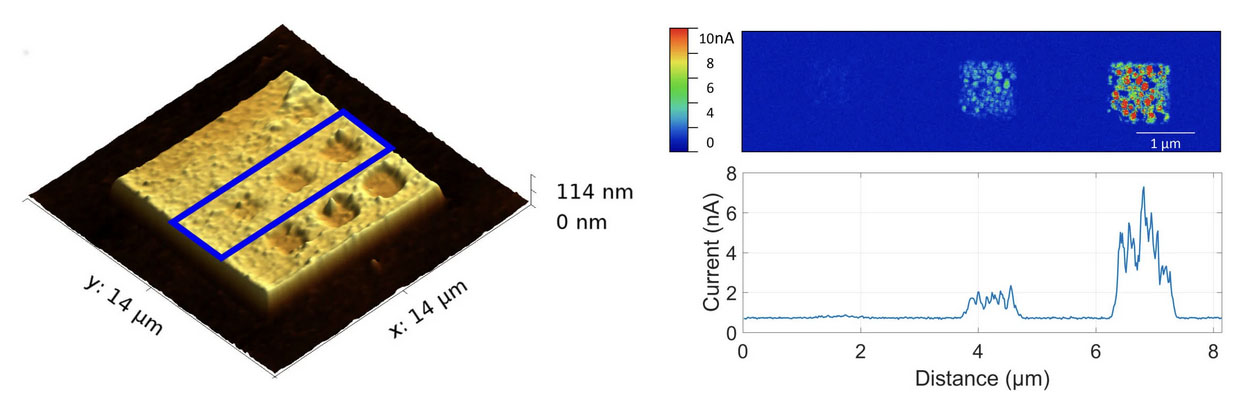
Conductive atomic force microscopy (C-AFM) is a powerful nanoscale characterization technique that combines the high-resolution imaging capabilities of atomic force microscopy (AFM) with the ability to measure electrical properties, such as conductivity, at the nanoscale. C-AFM allows researchers to simultaneously map the topography and local electrical properties of a sample, providing valuable insights into the structure-property relationships of nanomaterials and nanodevices.
Principle of Operation
In C-AFM, a conductive AFM probe, typically made of silicon or silicon nitride and coated with a thin metal layer (e.g., gold or platinum), is used to scan the sample surface. The probe is brought into contact with the sample, and a constant force is maintained between the probe and the sample using a feedback loop. A voltage is applied between the conductive probe and the sample, and the resulting current flowing through the probe-sample contact is measured using a sensitive current amplifier.
As the probe scans the sample surface, it simultaneously records the topography and the local electrical current at each point. This allows for the generation of high-resolution maps of the sample's topography and electrical properties, such as conductivity, resistance, or current-voltage characteristics.
Operating Modes
C-AFM can be operated in several modes, depending on the specific measurement requirements:
Contact Mode C-AFM
In contact mode C-AFM, the conductive probe is in direct contact with the sample surface, and a constant force is maintained between the probe and the sample. This mode is suitable for measuring the electrical properties of conductive and semiconductive samples, as well as for mapping the local conductivity variations across the sample surface.
Tapping Mode C-AFM
Tapping mode C-AFM, also known as intermittent contact mode, involves oscillating the conductive probe near its resonance frequency and maintaining a constant amplitude of oscillation. The probe intermittently contacts the sample surface, reducing lateral forces and minimizing sample damage. Tapping mode C-AFM is particularly useful for studying soft or delicate samples, such as organic semiconductors or biological materials.
Spectroscopic Modes
C-AFM can also be used in spectroscopic modes, where the probe is held stationary at a specific location on the sample, and the voltage is swept while measuring the resulting current. This allows for the acquisition of local current-voltage (I-V) characteristics, providing insights into the electronic properties of the sample, such as conductivity, carrier mobility, and energy barriers.
Applications of C-AFM
C-AFM has found widespread applications in various fields of nanotechnology, materials science, and nanoelectronics. Some key applications include:
- Nanoscale Electrical Characterization: C-AFM enables the electrical characterization of nanomaterials, such as nanowires, nanoparticles, and thin films, with nanometer-scale spatial resolution. It allows researchers to study the local electrical properties, such as conductivity, resistance, and carrier transport, at the nanoscale.
- Nanoelectronic Devices: C-AFM is extensively used in the characterization of nanoelectronic devices, such as transistors, memristors, and solar cells. It enables the mapping of local electrical properties, the identification of conductive pathways, and the study of charge transport mechanisms in these devices.
- Defect and Interface Analysis: C-AFM is a powerful tool for investigating defects, grain boundaries, and interfaces in nanomaterials and devices. It allows for the localization and characterization of electrically active defects, such as current leakage paths or conductive filaments, which can significantly impact device performance.
- Energy Storage and Conversion Materials: C-AFM is applied in the study of energy storage and conversion materials, such as battery electrodes, fuel cell catalysts, and thermoelectric materials. It enables the mapping of local conductivity variations, the identification of conductive phases, and the investigation of charge transport mechanisms in these materials.
Challenges and Limitations
While C-AFM offers unique capabilities for nanoscale electrical characterization, it also faces several challenges and limitations:
- Probe-Sample Contact: The quality of the electrical contact between the conductive probe and the sample is critical for accurate C-AFM measurements. Factors such as probe wear, sample contamination, and surface roughness can affect the contact resistance and lead to measurement artifacts.
- Sample Preparation: C-AFM requires samples to be electrically connected to a conductive substrate or electrode. Sample preparation, such as the deposition of conductive layers or the fabrication of electrical contacts, can be challenging for certain materials and devices.
- Interpretation of Results: The interpretation of C-AFM results can be complex, as the measured current depends on various factors, such as the probe-sample contact area, the local electronic properties of the sample, and the applied voltage. Careful analysis and modeling are often required to extract meaningful information from C-AFM data.
Future Perspectives
The field of C-AFM is continuously evolving, driven by advancements in probe technology, instrumentation, and data analysis techniques. Some key areas of future development include:
- High-Speed C-AFM: The development of high-speed C-AFM systems, capable of fast scanning and data acquisition, will enable the study of dynamic processes and the mapping of large sample areas with high throughput.
- Environmental C-AFM: The integration of C-AFM with environmental control capabilities, such as temperature and humidity control, will allow for the study of electrical properties under varying environmental conditions, relevant for practical device applications.
- Multimodal C-AFM: The combination of C-AFM with other AFM-based techniques, such as Kelvin probe force microscopy (KPFM) or piezoresponse force microscopy (PFM), will provide a more comprehensive understanding of the electrical, electromechanical, and surface potential properties of nanomaterials and devices.
As C-AFM continues to advance, it is expected to play an increasingly important role in the development and optimization of novel nanomaterials, nanoelectronic devices, and energy storage and conversion systems.
Further Reading
Nanomaterials, Conductive Atomic Force Microscopy of Semiconducting Transition Metal Dichalcogenides and Heterostructures
Energetic Materials Frontiers, Atomic force microscopy in energetic materials research: A review
