Electron Beam Induced Deposition (EBID): Nanoscale 3D Printing with Electrons
What is Electron Beam Induced Deposition?
Electron beam induced deposition (EBID) is a nanofabrication technique that uses a focused electron beam to deposit materials onto a substrate with nanometer-scale precision. It is essentially a form of 3D printing at the nanoscale, where the electron beam acts as a "pen" to directly write three-dimensional nanostructures.
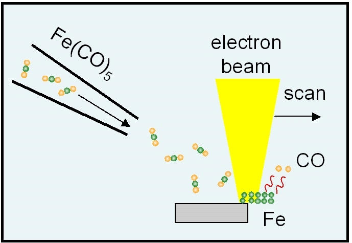
In EBID, a precursor gas, typically an organometallic compound, is introduced into the vacuum chamber of an electron microscope. The focused electron beam is then used to dissociate the precursor molecules adsorbed on the substrate surface. This causes the non-volatile part of the precursor to be deposited onto the substrate, while the volatile fragments are pumped away.
By controlling the position of the electron beam and the exposure time, intricate nanostructures can be fabricated with sub-10 nm resolution. EBID is capable of depositing a wide range of materials, including metals, semiconductors, and insulators.
Advantages of EBID
EBID offers several advantages over other nanofabrication techniques:
- High Resolution: EBID can achieve sub-10 nm feature sizes, making it one of the highest resolution additive nanofabrication techniques available.
- 3D Capability: Unlike planar lithography techniques, EBID can directly deposit material in three dimensions, enabling the fabrication of complex 3D nanostructures.
- Material Flexibility: EBID can deposit a wide range of materials by using different precursor gases, allowing for the fabrication of multimaterial nanostructures.
- Precise Positioning: The electron beam can be precisely positioned and focused, enabling the selective deposition of material at specific locations on a substrate.
Applications of EBID
EBID has found numerous applications in various fields of nanotechnology:
- Nanoelectronics: EBID can be used to fabricate nanoscale interconnects, electrodes, and contacts for nanoelectronic devices.
- Photonics: EBID enables the fabrication of nanophotonic structures, such as plasmonic antennas and waveguides, for manipulating light at the nanoscale.
- Sensors: EBID can be used to fabricate highly sensitive nanoscale sensors for chemical and biological detection.
- Catalysis: Nanostructures deposited by EBID can serve as catalysts for chemical reactions, taking advantage of their high surface-to-volume ratio.
- Micro- and Nanoelectromechanical Systems (MEMS/NEMS): EBID can be used to fabricate functional components for MEMS and NEMS devices, such as actuators and resonators.
Challenges and Future Perspectives
Despite its advantages, EBID still faces some challenges. One issue is the purity of the deposited material, as the decomposition of the precursor gas can lead to the incorporation of impurities. Researchers are developing new precursors and optimizing deposition parameters to improve the purity and quality of EBID-deposited materials.
Another challenge is the serial nature of EBID, which limits its throughput compared to parallel nanofabrication techniques. However, efforts are being made to develop multi-beam systems and optimize the deposition process to increase the speed and efficiency of EBID.
As EBID continues to evolve, it is expected to play an increasingly important role in the fabrication of advanced nanodevices and the realization of new nanoscale functionalities. The combination of EBID with other nanofabrication techniques, such as electron beam lithography and self-assembly, will open up new possibilities for creating complex, hierarchical nanostructures with unprecedented properties.
Further Reading
Nanomaterials, Pillar Growth by Focused Electron Beam-Induced Deposition Using a Bimetallic Precursor as Model System
Micromachines, Mechanical Properties of 3D Nanostructures Obtained by Focused Electron/Ion Beam-Induced Deposition: A Review
Journal of Applied Physics, 3D nanoprinting via focused electron beams
