| Posted: Jun 21, 2014 |
Formation of organic thin-film transistors through room-temperature printing |
| (Nanowerk News) Printed electronics, the field in which electronic devices are produced by printing functional materials in ink form without the need for large and expensive manufacturing equipment, has been drawing attention in recent years as a new technology for low-cost, large-area fabrication of semiconductor devices. By using plastic and other flexible substrates, the technology is expected to open paths for the mass production of devices by roll-to-roll processing or for new applications such as wearable devices. However, conventional printed electronics require many high-temperature processes ranging from 100 to 200°C. Because plastic substrates such as PET film generally have low heat resistance, there have been calls for the development of a low-temperature printing process that involves no high-temperature processes and that is applicable to a wide range of materials. However, such a process has not been realized to date. |
| In this research, the team established "room-temperature-printed electronics" by which electronics devices can be manufactured by conducting all of the printing processes at room temperature under ambient atmospheric conditions, without raising the temperature by even 1°C. Conventional printed electronics have mainly required high-temperature processes in order to sinter metal nanoparticle ink to be used as electrodes. Since conventional metal nanoparticles have used insulating materials as ligands for dispersing the nanoparticles in the ink, the nanoparticles have needed to be sintered in order to obtain a conductive metal film. |
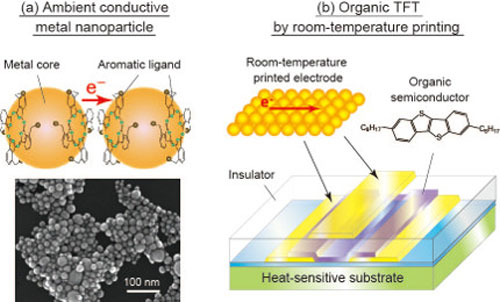 |
| Ambient conductive metal nanoparticles and an organic transistor created in this research: (a) Schematic and a scanning electron micrograph of ambient conductive metal nanoparticles. With the use of conductive aromatic ligands, the nanoparticles exhibit conductivity matching that of metal by room-temperature drying. (b) Schematic of an organic TFT formed by a room-temperature printing process. Since all layers of the TFT can be formed without raising the temperature by even 1°C, non-heat-resistant materials can also be used as substrates. It also exhibits extremely high mobility compared to conventional organic TFTs. (Image: National Institute for Materials Science) |
| In this research, the team succeeded in forming a metal film without post-coating sintering, by using conductive aromatic molecules as ligands of metal nanoparticles. The thin film obtained has achieved a resistivity of 9 × 10⁻⁶ Ω cm. In addition, by forming microscopic hydrophilic/hydrophobic patterns on the surface, the team patterned ambient conductive metal nanoparticles and organic semiconductors by a room-temperature process, and made organic thin-film transistors by forming all of the source and drain electrodes, organic semiconductors and gate electrodes by room-temperature printing. |
| Organic TFTs formed on a plastic substrate and a paper substrate respectively indicated an average mobility of 7.9 and 2.5 cm2 V-1 s-1. This value far exceeds the average mobility of amorphous silicon TFTs at 0.5 cm2 V-1 s-1 and almost matches the mobility of mass-produced IGZO TFTs (up to 10 cm2 V-1 s-1). |
| When manufacturing displays, etc. by printed electronics, circuits need to be printed on flexible substrates at a positional accuracy greater than several microns. Flexible plastic and paper substrates, which are weak against heat, became deformed or distorted under the conventional processing temperatures, leading to compromised accuracy. By conducting all of the manufacturing processes at room temperature, it will be possible to completely control the heat deformation of substrates and to print micro circuits at high accuracy. Furthermore, the production processes at room temperature under ambient atmospheric conditions would, in principle, enable the production of electronic devices on the surface of materials that are extremely weak against environmental changes, such as biomaterials. This achievement is expected to lead to applications in diverse fields including health care and bioelectronics. |
| These research results will be published in the journal Advanced Functional Materials in the near future. |
| Source: National Institute for Materials Science |

