| Posted: Aug 12, 2014 |
Researchers prove stability of silicene
|
|
(Nanowerk News) An international team of researchers has taken a significant step towards understanding the fundamental properties of the two-dimensional material silicene by showing that it can remain stable in the presence of oxygen.
|
|
In a study published today, 12 August, in IOP Publishing’s journal 2D Materials ("24 h stability of thick multilayer silicene in air"), the researchers have shown that thick multilayers of silicene can be isolated from parent material silicon and remain intact when exposed to air for at least 24 hours.
|
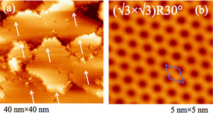 |
| Left: Filled-states STM topograph (40 × 40 nm2; V = -0.1 V, I = 0.16 nA) giving a bird's eye view of a multilayer silicene film (~10 MLs) grown at 470 K covering the entire scanned area in a single orientation, as indicated by the arrows; Right: zoom-in (5 × 5 nm2 showing the honeycomb (√3 × √3)R(30°) surface structure of each terrace (the √3 × √3 silicene cell is indicated). (© IoP)
|
|
It is the first time that such a feat has been achieved and will allow scientists to further probe the material and exploit the properties that have made silicene a promising material in the electronics industry.
|
|
Silicene is made from single honeycomb-shaped layers of silicon that are just one atom thick. At the moment, silicene must be produced in a vacuum to avoid any contact with oxygen, which could completely destroy the formation of the single layers.
|
|
Silicene must also be “grown” on a surface that matches its natural structure — silver is the leading candidate. To create silicene, a wafer of silicon is heated to high temperatures, forcing single silicon atoms to evaporate and land on the silver substrate, forming the single layer.
|
|
Silicene can also be transformed from a 2D material into a 3D material by stacking more and more single layers on top of each other. However, previous research has demonstrated that silicene has suicidal tendencies, and always reverts back to silicon as more layers are added, because a silicon structure is more stable.
|
|
In this new study, an international team of researchers based in Italy and France fabricated multilayers of silicene using a silver substrate kept at a temperature of 470 K and a solid silicon source, which was heated to 1470 K. A total of 43 monolayers of silicene were deposited onto the substrate.
|
|
Once fabricated, the researchers observed that a very thin layer of oxidation had formed on top of the multilayered stack of monolayers; however, it was shown that this preserved the integrity of the stack, acting like a protective layer.
|
|
The stack of monolayers remained preserved for at least 24 hours in open air, in which time the researchers were able to use x-ray diffraction and Raman spectroscopy to confirm that the material was in fact silicene and not ordinary silicon.
|
|
Lead author of the study Paola De Padova, from Consiglio Nazionale delle Ricerche in Italy, said: “These results are significant as we have shown that it is possible to obtain a silicon-based 2D material, which up until a couple of years ago was deemed inconceivable.
|
|
“Our present study shows that multilayered silicene is more conductive than single-layered silicene, and therefore opens up the possibility of using it throughout the silicon microelectronics industry. In particular, we envisage the material being used as gate in a silicene-based MOSFET, which is the most commonly used transistor in digital and analogue circuits.
|
|
“We are currently studying the possibility of growing multilayered silicene directly onto semiconductor substrates to explore the joint superconducting properties.”
|

