| Posted: Mar 07, 2016 |
Warming up optoelectronic research(Nanowerk News) A team of physicists from the University of California, San Diego and The University of Manchester is creating tailor-made materials for cutting-edge research and perhaps a new generation of optoelectronic devices. The materials make it easier for the researchers to manipulate excitons, which are pairs of an electron and an electron hole bound to each other by an electrostatic force. |
| Excitons are created when a laser is shone onto a semiconductor device. They can transport energy without transporting net electric charge. Inside the device the excitons interact with each other and their surroundings, and then convert back into light. This makes them attractive for new technology. Inside the device the excitons interact with each other and their surroundings, and then convert back into light that can be detected by extremely sensitive charge-coupled device (CCD) cameras. |
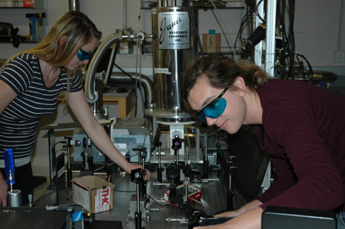 |
| Erica Calman and Chelsey Dorow align optics required to collect measurements from a molybdenum disulfide sample. |
| Most of the team’s previous work involved structures based on gallium arsenide (GaAs), which is a material commonly used throughout the semiconductor industry. Unfortunately, the devices they’ve developed come with a fundamental limitation: They require cryogenic temperatures (below 100 K) -- ruling out any commercial applications. |
| So the team made a radical material change to bring their excitonic devices up to room temperature. They report their results in Applied Physics Letters ("Control of excitons in multi-layer van der Waals heterostructures"). |
| “Our previous structures were built from thin layers of GaAs deposited on top of a substrate with a particular layer thickness and sequence to ensure the specific properties we wanted,” said Erica Calman, lead author and a graduate student in the Department of Physics, University of California, San Diego. |
| To make the new devices the physicists turned to new structures built from a specially designed set of ultrathin layers of materials -- molybdenum disulfide (MoS2) and hexagonal boron nitride (hBN) -- each a single atom thick. |
| These structures are produced via the famous “Scotch tape” or mechanical exfoliation method developed by the group of Andre Geim, a physicist awarded a Nobel Prize in physics in 2010 for his groundbreaking work regarding the two-dimensional material graphene. |
| “Our specially designed structures help keep excitons bound more tightly together so that they can survive at room temperature -- where GaAs excitons are torn apart,” explains Calman. |
| Impressively, excitons can form a special quantum state known as a Bose-Einstein condensate. This state occurs within superfluids and enables currents of particles without losses. The team discovered a similar exciton phenomenon at cold temperatures with GaAs materials. |
| “The results of our work suggest that we may be able to make new structures work all the way up to room temperature,” said Calman. “We set out to prove that we could control the emission of neutral and charged excitations by voltage, temperature, and laser power … and demonstrated just that.” |
| Source: American Institute of Physics |

