| Posted: Oct 05, 2018 |
Atomically thin, part-organic semiconductor for bendable phones(Nanowerk News) Engineers at ANU have invented a semiconductor with organic and inorganic materials that can convert electricity into light very efficiently, and it is thin and flexible enough to help make devices such as mobile phones bendable (Advanced Materials, "Efficient and Layer-Dependent Exciton Pumping across Atomically Thin Organic–Inorganic Type-I Heterostructures"). |
| The invention also opens the door to a new generation of high-performance electronic devices made with organic materials that will be biodegradable or that can be easily recycled, promising to help substantially reduce e-waste. |
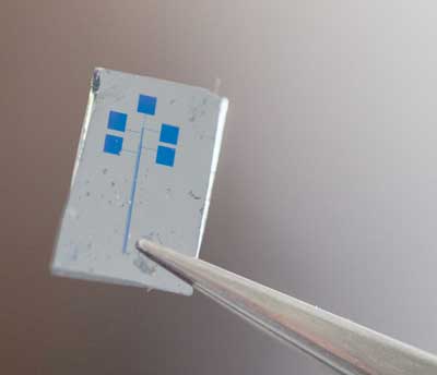 |
| The semiconducting material, which cannot be seen with the naked eye, sits in between gold electrodes on the chip (pictured) that is a functional transistor. The chip can hold close to a thousand transistor circuits. (Image: Jack Fox, ANU) |
| The huge volumes of e-waste generated by discarded electronic devices around the world is causing irreversible damage to the environment. Australia produces 200,000 tonnes of e-waste every year - only four per cent of this waste is recycled. |
| The organic component has the thickness of just one atom - made from just carbon and hydrogen - and forms part of the semiconductor that the ANU team developed. The inorganic component has the thickness of around two atoms. The hybrid structure can convert electricity into light efficiently for displays on mobile phones, televisions and other electronic devices. |
| Lead senior researcher Associate Professor Larry Lu said the invention was a major breakthrough in the field. |
| "For the first time, we have developed an ultra-thin electronics component with excellent semiconducting properties that is an organic-inorganic hybrid structure and thin and flexible enough for future technologies, such as bendable mobile phones and display screens," said Associate Professor Lu from the ANU Research School of Engineering. |
| PhD researcher Ankur Sharma, who recently won the ANU 3-Minute Thesis competition, said experiments demonstrated the performance of their semiconductor would be much more efficient than conventional semiconductors made with inorganic materials such as silicon. |
| "We have the potential with this semiconductor to make mobile phones as powerful as today's supercomputers," said Mr Sharma from the ANU Research School of Engineering. |
| "The light emission from our semiconducting structure is very sharp, so it can be used for high-resolution displays and, since the materials are ultra-thin, they have the flexibility to be made into bendable screens and mobile phones in the near future." |
| The team grew the organic semiconductor component molecule by molecule, in a similar way to 3D printing. The process is called chemical vapour deposition. |
| "We characterised the opto-electronic and electrical properties of our invention to confirm the tremendous potential of it to be used as a future semiconductor component," Associate Professor Lu said. |
| "We are working on growing our semiconductor component on a large scale, so it can be commercialised in collaboration with prospective industry partners." |
| Source: Australian National University |
|
Subscribe to a free copy of one of our daily Nanowerk Newsletter Email Digests with a compilation of all of the day's news. |

