| May 23, 2019 |
New Flatland material: Physicists obtain quasi-2D gold(Nanowerk News) Researchers from the MIPT Center for Photonics and 2D Materials have synthesized a quasi-2D gold film, showing how materials not usually classified as two-dimensional can form atomically thin layers. |
| Published in Advanced Material Interfaces ("Ultrathin and ultrasmooth gold films on monolayer MoS2"), the study shows that by using monolayer molybdenum disulfide as an adhesion layer, quasi-2D gold can be deposited on an arbitrary surface. The team says the resulting ultrathin gold films, which are just several nanometers thick, conduct electricity very well and are useful for flexible and transparent electronics. |
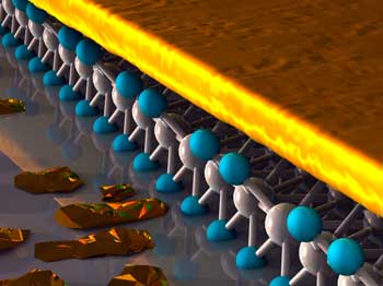 |
| Quasi-two-dimensional gold. (Image: Ella Maru Studio) |
| The advent of 2D metals brings us closer to a new class of optical metamaterials whose unique potential to control light could lead to unexpected technologies, such as Harry Potter’s invisibility cloak. |
| The first 2D material to be discovered, graphene is a one-atom-thick sheet of carbon atoms in a honeycomb formation. Its synthesis and the study of its exciting properties have given rise to an entirely new field of science and technology. The “groundbreaking experiments regarding the two-dimensional material” earned MIPT graduates Andre Geim and Kostya Novoselov the 2010 Nobel Prize in physics. |
| Since graphene opened up a brand-new world of 2D materials, more than 100 of its cousins have been discovered. Their intriguing properties lead to applications in fields ranging from biomedicine and electronics to the aerospace industry. These materials belong to the class of layered crystals, whose layers are weakly bound to one another but have strong internal integrity. For example, the graphite in a pencil is essentially many stacked-up layers of graphene, bound so weakly that Geim and Novoselov famously used sticky tape to peel them off. |
| However, many materials — like the metals gold, silver, and copper — do not have a layered structure. Still, they could theoretically form 2D layers, which would be indispensable for flexible and transparent electronics: folding displays, e-paper and e-clothing, lenses with built-in electronics, etc. Among the possible applications are even ultrathin electrodes that would enable neural interfaces with potential to solve medical problems and eventually integrate the nervous system of a living being with electronic devices. |
| Until recently, the only technology for depositing metal films on arbitrary surfaces yielded layers that were not thin enough. It involves thermally evaporating a 3D metal sample in high vacuum. The evaporated metal particles then adhere to a silicon-based substrate, forming nanosized islands, which gradually grow, eventually closing the gaps between them. |
| This process yields relatively homogeneous films only by the time they are 20 nanometers thick. Yet engineers require transparent films, which means they need to be more than two times thinner. Stopping the deposition earlier is not an option either, because the films still have too many gaps and inhomogeneities (see the lower right image in Figure 3), impairing their electrical conductivity. Similarly, a metal mesh is a worse conductor compared with a sheet of metal. |
| The researchers from the Moscow Institute of Physics and Technology began by hypothesizing that 2D metals could be deposited on other 2D materials. Graphene was the first candidate, but gold exhibited poor wetting to it. As a result, gold was deposited in the form of pillars. This vertical mode of growth made closing the gaps in the film problematic. Although gold deposition on graphene is interesting for other applications, such as surface-enhanced Raman spectroscopy, the sub-10-nanometer films obtained in this way do not conduct electricity. |
| The team went on to investigate metal film growth on 2D transition metal dichalcogenides. Specifically, molybdenum disulfide was used, because sulfur compounds are known to be among the very few to form stable bonds with gold. |
| “We have had that idea for quite some time. However, many of the technologies for working with 2D materials are still in development. Not all of them are widely available,” explained Yury Stebunov, one of the lead authors of the paper. “This study required substantial resources, both human and material. It is by securing a grant under the presidential program that we could put our ideas into practice.” |
 |
| Figure 2. The method used in the study: Gold (Au) is deposited on a monolayer of molybdenum disulfide (MoS2), which rests upon a silicon (Si) substrate with an oxidized layer labeled SiO2; “vdW gap” denotes the van der Waals gap. (Image: MIPT) |
| The MIPT researchers used thermal evaporation in high vacuum to deposit thin gold films on a silicon substrate covered with silicon dioxide and a monolayer of molybdenum disulfide (figure 2). The team employed electron and atomic force microscopy to compare the structure of these gold films at various thicknesses to analogous films grown on pure silicon dioxide — that is, without the molybdenum disulfide monolayer (figure 3). The added 2D material interface resulted in continuous gold films with superior electrical conductivity at a lesser thickness of merely 3-4 nanometers. |
| Since photonic and optoelectronic devices are a key application of such quasi-2D metal films, the physicists studied the optical properties of their samples via spectral ellipsometry, reporting for the first time the optical constants for ultrathin gold films. |
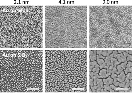 |
| Figure 3. Gold films (Au) of varying thickness — indicated in nanometers (nm) — deposited on the conventionally used silicon dioxide substrate (SiO2, bottom row) and a molybdenum disulfide monolayer (MoS2, top row), as seen with an electron microscope. Image courtesy of the researchers |
| The paper’s senior author, professor Valentyn Volkov of the University of Southern Denmark, who also heads the Laboratory of Nanooptics and Plasmonics at MIPT, commented: “Any researcher can use our data to model photonic or optoelectronic devices or even the artificial materials also known as metamaterials. Eventually, the technology we proposed can help to design such materials and devices.” |
| A single added layer of molybdenum disulfide enabled record-thin and smooth metal films. The team emphasizes the universal applicability of their technique: The monolayer can be deposited on an arbitrary surface with any properties to produce an ultrathin, ultrasmooth metal film coating. Such quasi-2D metal layers can be integrated into multilayer “sandwich” structures incorporating various 2D materials. Known as van der Waals heterostructures, they might feature diverse “ingredients,” including semiconductors, dielectrics, semimetals, and — from now on — metals, too. |
| A co-author of the study, Aleksey Arsenin, who heads the Center for Photonics and 2D Materials at MIPT, added: “We expect that this is merely the beginning of quasi-2D metal science. A while ago, these materials were inaccessible even to scientists. With our technology, we can talk about the prospects they hold for flexible and transparent electronics. Hopefully, we will soon see it in production.” |
| Source: Moscow Institute of Physics and Technology |
|
Subscribe to a free copy of one of our daily Nanowerk Newsletter Email Digests with a compilation of all of the day's news. |

