| Dec 10, 2021 |
Development of a high-energy-resolution, LaB6 nanowire-based field emission gun(Nanowerk News) The National Institute for Materials Science (NIMS) and JEOL, Ltd. have developed a lanthanum hexaboride (LaB6) nanowire-based field emission gun that is installable on an aberration-corrected transmission electron microscope (TEM). |
| This combined unit is able to perform atomic resolution observation at an energy resolution of 0.2 eV—the highest resolution ever recorded for non-monochromatic electron guns—with a high current stability of 0.4% (Nature Nanotechnology, "High-endurance Micro-engineered LaB6 Nanowire Electron Source for High-resolution Electron Microscopy"). |
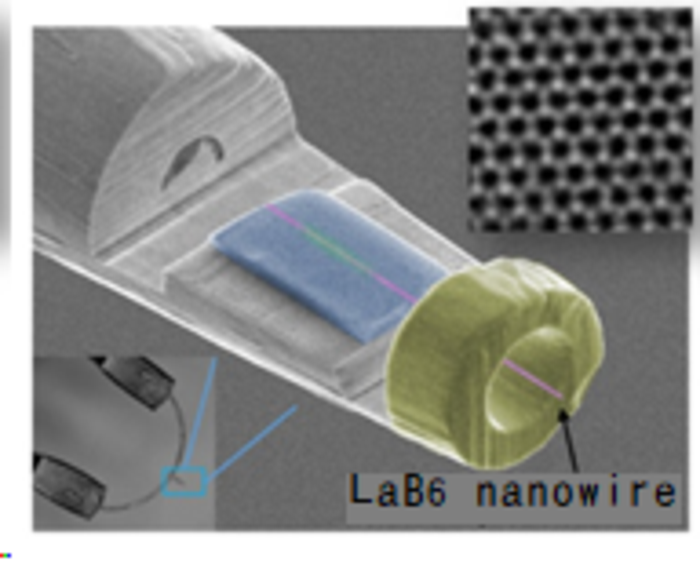 |
| SEM image of the LaB6 nanowire-based electron source. An atomic resolution image of single-layer graphene taken by a TEM equipped with this electron source is shown in the boxed image at upper right. (Image: Koji Kimoto, National Institute for Materials Science) |
| Unsuccessful efforts have been made for more than 20 years to develop field emission guns using theoretically high-performance nano materials. It has been found challenging to integrate a nanowire-based field emission gun into an electron microscope without undermining its physical properties, such as lives and stability. For this reason, commercially available field emission guns are still equipped with tungsten needles developed more than half a century ago. |
| This NIMS-JEOL research team 1) developed techniques to chemically synthesize and grow high-purity, single-crystal nanowires of LaB6, known to be an excellent electron-emitting hot cathode material, 2) designed an electron source mechanism capable of efficiently emitting electrons and 3) developed techniques to extract a single nanowire and integrate it into an optimized electron source structure. |
| The LaB6 nanowire-based electron source has a number of advantages: relatively moderate vacuum condition requirements, very high current stability, low extraction voltage, narrow electron beam energy distribution width and high brightness. This electron source may be applicable to the development of next-generation field emission electron microscopes with higher spatial and energy resolution—potentially valuable tools in the semiconductor and medical fields. |
| Source: National Institute for Materials Science, Japan |

