| May 21, 2012 |
Cloak and swagger: Engineers use plasmonics to create an invisible photodetector
|
|
(Nanowerk News) It may not be intuitive, but a coating of reflective metal can actually make something less visible, engineers at Stanford and UPenn have shown. They have created an invisible, light-detecting device that can "see without being seen."
|
|
At the heart of the device are silicon nanowires covered by a thin cap of gold. By adjusting the ratio of metal to silicon – a technique the engineers refer to as tuning the geometries – they capitalize on favorable nanoscale physics in which the reflected light from the two materials cancel each other to make the device invisible.
|
|
Pengyu Fan is the lead author of a paper demonstrating the new device published online May 20th in the journal Nature Photonics ("An invisible metal–semiconductor photodetector"). He is a doctoral candidate in materials science and engineering at Stanford University working in Professor Mark Brongersma's group. Brongersma is senior author of the study.
|
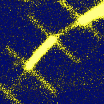 |
| An image showing light scattering from a silicon nanowire running diagonally from bottom left to top right. The brighter areas are bare silicon while the dimmer sections are coated with gold demonstrating how plasmonic cloaking reduces light scattering in the gold-coated sections. (Photo: Stanford Nanocharacterization Lab)
|
|
Cloak of invisiblity
|
|
Light detection is well known and relatively simple. Silicon generates electrical current when illuminated and is common in solar panels and light sensors today. The Stanford device, however, is a departure in that for the first time it uses a relatively new concept known as plasmonic cloaking to render the device invisible.
|
|
The field of plasmonics studies how light interacts with metal nanostructures and induces tiny oscillating electrical currents along the surfaces of the metal and the semiconductor. These currents, in turn, produce scattered light waves.
|
|
By carefully designing their device – by tuning the geometries – the engineers have created a plasmonic cloak in which the scattered light from the metal and semiconductor cancel each other perfectly through a phenomenon known as destructive interference.
|
|
The rippling light waves in the metal and semiconductor create a separation of positive and negative charges in the materials – a dipole moment, in technical terms. The key is to create a dipole in the gold that is equal in strength but opposite in sign to the dipole in the silicon. When equally strong positive and negative dipoles meet, they cancel each other and the system becomes invisible.
|
|
"We found that a carefully engineered gold shell dramatically alters the optical response of the silicon nanowire," said Fan. "Light absorption in the wire drops slightly – by a factor of just four – but the scattering of light drops by 100 times due to the cloaking effect, becoming invisible."
|
|
"It seems counterintuitive," said Brongersma, "but you can cover a semiconductor with metal – even one as reflective as gold – and still have the light get through to the silicon. As we show, the metal not only allows the light to reach the silicon where we can detect the current generated, but it makes the wire invisible, too."
|
|
Broadly effective
|
|
The engineers have shown that plasmonic cloaking is effective across much of the visible spectrum of light and that the effect works regardless of the angle of incoming light or the shape and placement of the metal-covered nanowires in the device. They likewise demonstrate that other metals commonly used in computer chips, like aluminum and copper, work just as well as gold.
|
|
To produce invisibility, what matters above all is the tuning of metal and semiconductor.
|
|
"If the dipoles do not align properly, the cloaking effect is lessened, or even lost," said Fan. "Having the right amount of materials at the nanoscale, therefore, is key to producing the greatest degree of cloaking."
|
|
In the future, the engineers foresee application for such tunable, metal-semiconductor devices in many relevant areas, including solar cells, sensors, solid-state lighting, chip-scale lasers, and more.
|
|
In digital cameras and advanced imaging systems, for instance, plasmonically cloaked pixels might reduce the disruptive cross-talk between neighboring pixels that produces blur. It could therefore lead to sharper, more accurate photos and medical images.
|
|
"We can even imagine reengineering existing opto-electronic devices to incorporate valuable new functions and to achieve sensor densities not possible today," concluded Brongersma. "There are many emerging opportunities for these photonic building blocks."
|
|
Brongersma lab alumnus Professor Linyou Cao and doctoral candidate Farzaneh Afshinmanesh contributed to this research. This work is a collaboration with Professor Nader Engheta and post-doctoral researcher Uday Chettiar from University of Pennsylvania.
|

