| Posted: October 29, 2008 |
New assembly technique for three-dimensional carbon nanotube structures |
|
(Nanowerk News) Srinivas Sridhar, Ph.D., distinguished professor and chair of Physics at Northeastern University, Evin Gultepe and their team of researchers from the university’s Electronic Materials Research Institute have demonstrated a technique to assemble single-walled carbon nanotubes (SWNT) into three-dimensional structures. This technique will be useful for the large scale, accelerated assembly of SWNTs at room temperature, which is more suitable for nanoscale electronic applications, such as flat panel displays and electronic memory devices.
|
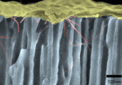 |
| A cross-sectional view of SEM micrographs of assembled SWNTs in anodic alumina array fabricated on Silican
|
|
This research was published in an October 2008 issue of the journal Nanotechnology.
|
|
The electronic properties of SWNTs, such as large current capacities and quick mobility, makes them one of the most highly researched structures for the development of nanoscale electronics. They are able to conduct energy more quickly and efficiently than current structures and provide a platform from which to build smaller-scale products. Widely used materials, such as copper, do not meet the requirements as effective electrical interconnects on a smaller scale.
|
|
The challenge of utilizing carbon nanotubes (CNT) in the nanoscale is to assemble them into three-dimensional structures for large scale applications. Currently, manufacturing CNTs requires growing or assembling them into a device, which requires very hot temperatures and complex post-assembly procedures. In contrast, a post-synthesis assembly method allows for the arrangement of CNTs in ambient temperatures, which gives more flexibility in the manufacturing process.
|
|
In this newly discovered process, Gultepe, Sridhar and their colleagues manufactured nanotemplates, with billions of nano-sized holes in which to house the SWNTs. Utilizing electrical fields, they were able assemble the SWNTs vertically into the alumina nanotemplate, with a silican substrate bottom layer and a metal top layer. The vertically-assembled three-dimensional SWNTs provide the electrical interconnection between the nanotemplates and the silicon substrates.
|
|
“The greatest significance of this process is the potential to manufacture three-dimensional SWNTs electrical interconnects at a high-rate and on a larger scale,” said Sridhar, who is also the Director of the Electronic Materials Research Institute at Northeastern. “Scaling down the nominal feature size means greater performance and decreased costs.”
|
|
In addition to Sridhar, the team of researches involved with this project includes Ahmed Busnaina, Ph.D., Director of Northeastern’s Center for High-rate Nanomanufacturing, Dattatri Nagesha, Ph.D., Bernard Diddier Frederic Casse, Ph.D., and Selvapraba Selvarasah. This research was supported by the IGERT Nanomedicine Science and Technology and the NSF Nanoscale Science and Engineering Centers Program.
|
|
For more information about Professor Sridhar’s research, please contact Jenny Eriksen at (617) 373-2802 or via email at [email protected].
|

