| Mar 06, 2014 |
Using carbon to control light at the nanoscale
|
|
(Nanowerk News) The flip of a light switch – a nanoscale light switch – may some day dramatically boost the speed of data transmission, from streaming movies to accelerating the most data-intense computation. Today, information flow in a computer is based on electrical pulses. But if an electrical signal could instead control a light switch, the “ones and zeros” that give data meaning could race through computer circuits at ten times the current speed. A ten-fold increase in speed would mean a similar spike in the volume of information that can be processed.
|
|
Of course, electrical signals are used to modulate light in the optical fibers that transmit massive amounts of data around the corner and around the world. But harnessing light to boost communication between chips within a computer circuit has proved an elusive goal. At the scale of computer circuitry, materials such as silicon can’t absorb light efficiently, and devices that can perform well are too bulky to integrate into a chip.
|
|
So excitement runs high that graphene, a material under intense study for only a decade, might do the trick. Single atom-thick carbon graphene crystals absorb all wavelengths of light, and at certain voltages, electrical pulses can turn the material’s light absorption on and off – the key to data transmission. This trait and graphene’s nano-size “footprint” make it an ideal candidate for ultra-miniature optical devices that could be installed by the thousands on a chip to control traffic flow.
|
|
“We’re not there yet,” says Feng Wang, assistant professor of physics and a Bakar Fellow, “but graphene’s remarkable combination of electrical and optical properties, and its potential for nanofabrication hold great promise for optoelectronics.”
|
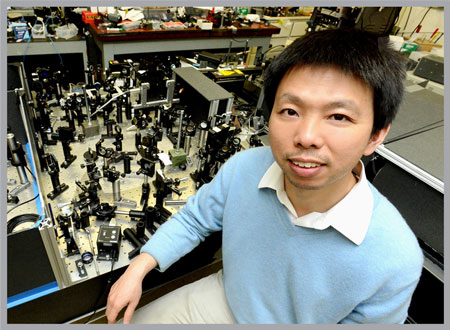 |
| eng Wang performing optoelectronic measurements in the lab.
|
|
Wang’s lab studies how electrical fields modulate the optical properties of a number of materials. The Bakar Fellows Program supports his efforts to develop graphene modulators for chip-to-chip communication. Because he’s manipulating photons, he can do much of the research under an optical microscope. At this relatively low magnification, a graphene layer looks like a continuous thin sheet. But under the power of a scanning tunneling microscope that can resolve individual atoms, the material’s chicken wire-like atomic configuration appears.
|
|
Wang grew up in Nanchang in the south of China and went to college in Shanghai. He received his PhD in physics at Columbia and was a postdoc at Berkeley before joining the physics faculty. His focus on graphene’s potential to boost chip-to-chip performance in computers circuits began about six years ago. Before that, he studied carbon nanotubes, a one dimensional carbon material.
|
|
"Our lab mainly focuses on the fundamental physics of how light interacts with materials at the nano-scale, and what novel properties emerge,” Wang says. This holds a lot of fascination for me.
|
|
“But exploring ways to exploit some of these novel behaviors in microelectronics is just as exciting. The basic research can reveal real-world applications. It’s a great combination.”
|
|
Out on the horizon, Wang can see graphene integrated into infrared imagers and optical sensors, and possibly being used to detect telltale changes in diseased cells. Metabolism changes the pH, or acidity, of cells, and fast-metabolizing cancer cells have distinct metabolic signatures. Local pH variations, in turn, alter the optical absorption properties of graphene. This could be measured to aid in diagnosis.
|
|
Similarly, graphene may one day aid detection of neurological disease. Neurons communicate with pulses of ions – their so-called “action potential” – and the release of ions modified the optical absorption of graphene. Such a change in graphene could potentially be used detect neuron activity.
|
|
These applications are well down the line, Wang says, though not at all out of the question. For now, he seems fully absorbed by the physics of this truly absorbing nanomaterial.
|

