Showing Spotlights 1177 - 1184 of 2785 in category All (newest first):
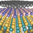 Much hope (and hype) rides on graphene as a 'post-silicon' material for fabricating next-generation nanoelectronic devices. However, graphene's Achilles heel is its lack of an energy band gap. Therefore, graphene must be modified to produce a band gap, if it is to be used in electronic devices. Using a new approach, researchers now have demonstrated the operation of an all two-dimensional transistor, using a transition metal dichalcogenides channel material, hexagonal boron nitride gate dielectric, and graphene source/drain and gate contacts.
May 13th, 2014
 The growing market of power electronics creates new challenges for engineers and material specialists as it requires devices withstanding increasingly high voltages and for this new approaches to design and the adoption of new materials such as gallium nitride (GaN) and silicon carbide (SiC) are needed. The biggest point of attention for power electronics is breakdown voltage, that is, the highest voltage applicable to the device before it breaks down and starts to become non-functional.
May 12th, 2014
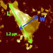 The way graphene sheets are produced in solution, by exfoliation, is an original process, still not completely understood. The exfoliation of a 2D object from a 3D bulk material is a process spanning from the nano- to meso-scale due to bubble cavitation, intercalation and disruptive fragmentation. When characterizing these 2D sheet solutions, their average size and size standard deviation are commonly reported, often assuming that their size follows a 'normal' distribution. Experimental data shows that this is not the case.
May 8th, 2014
 For years, scientists and engineers have worked to design electronics which can interface with the body. However, typical silicon wafer-based electronics, which are planar and stiff, are not suited to interface with the soft, curvilinear, and dynamic environment that biology presents. By exploiting the features of shape-memory polymer (SMP) substrates, an international team of researchers has now demonstrated a unique form of adaptive electronics which softly conform or deploy into 3D shapes after exposure to a stimulus. The resulting organic thin-film transistors (OTFTs) can change their mechanical properties from rigid and planar, to soft and compliant, in order to enable soft and conformal wrapping around 3D objects, including biological tissue.
May 7th, 2014
 The development of sustainable, robust, energy-efficient and cost-effective water purification technologies is a challenging task. Conventional practices adopted for water purification suffer from certain limitations such as high cost, low adsorption capacity, generation of toxic sludge, etc. A possible solution to tackle this problem has been demonstrated by scientists in India. They developed nanotechnology-based water purification using nano-silica-silver composite material as antifouling, antimicrobial and dye adsorptive material.
May 6th, 2014
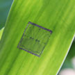 Taking the approach of flexible electronics one step further, researchers now have integrated all-carbon based electronic devices to live plants and insects. They developed an unconventional approach for the in situ synthesis of monolithically integrated electronic devices based on single-walled carbon nanotube channels and graphitic electrodes. The highly flexible transistors were formed directly by the in situ synthesis using patterned metal catalyst films and subsequently could be transferred to both planar and nonplanar substrates, including papers, clothes, and fingernails.
May 2nd, 2014
 Prevention and treatment of neurological disorders in humans necessitate delivery of therapeutic or neuroprotective agents across the so-called blood-brain barrier (BBB) into the brain. The scarcity of techniques for brain-specific delivery of therapeutic molecules using non-invasive approaches has led researchers to increasingly explore the promising potential of nanotechnology toward the diagnosis and treatment of diseases/disorders incurable with present techniques. A recent example of these efforts is the research to analyze the intra- and intercellular transport and fate of novel nanoparticles for drug delivery to the central nervous system.
May 1st, 2014
 Graphene's piezoresistive effect, combined with its other properties such as ultra-translucency, superior mechanical flexibility and stability, high restorability, and carrier mobility, enables the use of graphene in high-sensitivity strain sensors. Potential application areas for these sensors could be found in flexible display technology, robotics, smart clothing, electronic skin, in vitro diagnostics, implantable devices, and human physiological motion detection - which has been considered as an effective approach to evaluate human health. To demonstrate this application, researchers have now reported on a method to monitor human motions.
Apr 30th, 2014
 Subscribe to our Nanotechnology Spotlight feed