Showing Spotlights 1289 - 1296 of 2786 in category All (newest first):
 In contrast to flexible electronics, which rely on bendable substrates, truly foldable electronics require a foldable substrate with a very stable conductor that can withstand folding, i.e. an edge in the substrate at the point of the fold, which develops creases, and the deformation remains even after unfolding. That means that, in addition to a foldable substrate like paper, the conductor that is deposited on this substrate also needs to be foldable. Researchers have now demonstrated a fabrication process for foldable graphene circuits based on paper substrates.
Aug 22nd, 2013
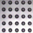 Graphene has a unique combination of properties that is ideal for next-generation electronics, including mechanical flexibility, high electrical conductivity, and chemical stability. Combine this with inkjet printing, already extensively demonstrated with conductive metal nanoparticle ink, and you get an inexpensive and scalable path for exploiting these properties in real-world technologies. Although liquid-phase graphene dispersions have been demonstrated, researchers are still struggling with sophisticated inkjet printing technologies that allow efficient and reliable mass production of high-quality graphene patterns for practical applications. Recent work has addressed these issues and proposes an approach to overcome these problems.
Aug 20th, 2013
 Vault particles are large, barrel-shaped nanoparticles found in the cytoplasm of all mammalian cells. All human cells so far analyzed have been shown to contain vaults with quantities varying from a few thousand per cell to in excess of 100 000 per cell. As naturally occurring nanoscale capsules, vaults may be useful to engineer as therapeutic delivery vehicles. The particles can be produced in large quantities and are assembled in situ from multiple copies of the single structural protein following expression. Using molecular engineering, recombinant vaults can be functionally modified and targeted, and their contents can be controlled by packaging.
Aug 19th, 2013
 Researchers fabricated nanoporous glass films using nanocrystals of cellulose, the main component of pulp and paper. The unique, helical structure of cellulose is replicated in a mineral. This helical organization synthetically mimics the structure of the exoskeletons of some iridescent beetles. Introducing porosity into photonic crystals provides a means to tune their optical properties by infiltrating the pores with various guests: When certain liquids are added to the film, the liquid gets trapped in the pores and changes the optical properties of the films.
Aug 15th, 2013
 With missing data about the large scale impact of nanotechnology, life cycle assessments of potential nanoproducts should form an integral part of nanotechnology research at early stages of decision making as it can help in the screening of different process alternatives. So far, however, life cycle studies of emerging nanotechnologies have been susceptible to huge uncertainties due to issues of data quality and the rapidly evolving nature of the production processes. A recent paper investigates the suitability of the U.S. regulatory system as a comprehensive package addressing multiple types and uses of engineered nanomaterials over their life cycle.
Aug 13th, 2013
 For a long time, scientists have been fascinated by the dramatic changes in color used by marine creatures like squids and octopuses, but they never quite understood the mechanism responsible for this. Only recently they found out that a neurotransmitter, acetylcholine, sets in motion a cascade of events that culminate in the addition of phosphate groups to a family of unique proteins called reflectins. Having begun to unravel the natural mechanisms behind these amazing abilities, researchers are trying to use this knowledge to make artificial camouflage coatings. New work addresses the challenge of making something appear and disappear when visualized with standard infrared detection equipment.
Aug 12th, 2013
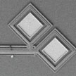 Semiconductor fabs are large, complex industrial sites with costs for a single facility approaching $10B. In this article we discuss the possibility of putting the entire functionality of such a fab onto a single silicon chip. We demonstrate a path forward where, for certain applications, especially at the nanometer scale, one might consider using a single chip approach for building devices, both integrated circuits and nano-electromechanical systems. Such methods could mean shorter device development and fabrication times with a significant potential for cost savings.
Aug 8th, 2013
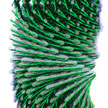
 With the semiconductor industry still on the path of Moore's law, researchers have already been toying with single-molecule electronics and molecular memory to push miniaturization of electronics to its limit. However, with electrical gadgets and devices getting increasingly smaller and functionally more powerful, the current density flowing through the copper and gold conductors in these devices has been exponentially increasing. Therefore, electrical conductors with higher current density tolerance are in huge demand and recent research has addressed this issue.
Aug 6th, 2013
 Subscribe to our Nanotechnology Spotlight feed