Showing Spotlights 1873 - 1880 of 2785 in category All (newest first):
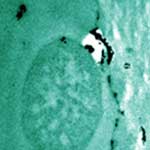 Some scientists believe that, with the increased mass production of engineered nanoparticles like carbon nanotubes, there is a realistic chance for these particles to interact with water, soil and air, and subsequently enter the food chain. However, understanding the behavior and impacts of nanomaterials in the environment and in human health is a daunting task. Nevertheless, a general understanding about nanotoxicity is slowly emerging as the body of research on cytotoxicity, genotoxicity, and ecotoxicity of nanomaterials grows. In our Spotlight today we take a look at new biophysical research - a parallel study of carbon-nanoparticle uptake by plant and mammalian cells - that contributes to the general picture of the fundamental behaviors of nanoparticles in both biological and ecological systems.
Mar 10th, 2010
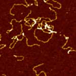 Imaging soft biological samples in liquid with Atomic Force Microscope has long stood as a very challenging task. Until recently, most of the works in this field has been carried out in tapping mode AFM, during which the cantilever driven by a piezoelectric actuator vibrates in the vicinity of the cantilever's resonance frequency, and briefly touches the sample surface at the bottom of each vibration cycle, resulting in a decrease of its oscillation amplitude. By keeping such amplitude at a preset value using feedback control, a topographic image of the sample surface is obtained. However, stable, high-resolution imaging of very fragile and sensitive biological samples such as live cells or individual proteins is not trivial in tapping mode due to potential sample distortion or even damage during the brief contact between the AFM tip and sample surface at the end of each oscillation cycle. The XE-series AFM with Crosstalk Elimination and high force Z-scanner has successfully solved these problems.
Mar 9th, 2010
 Spectrometers are used in materials analysis by measuring the absorption of light by a surface or chemical substance. These instruments measure properties of light over a specific portion of the electromagnetic spectrum. In conventional spectrometers, a diffraction grating splits the light source into several beams with different propagation directions according to the wavelength of the light. Thus, to achieve sufficient spatial separation for intensity measurements at a small slit, a long light path - i.e., a large instrument - is required. However, for lab-on-a-chip applications, the spectrometer must be integrated into a sub-centimeter scale device to produce a stand-alone platform. To achieve this, researchers at the Korea Advanced Institute of Science and Technology (KAIST) propose a new paradigm in which the spectrometer is based on an array of photonic crystals with different bandgaps.
Mar 8th, 2010
 Surface energy is ubiquitous in nature and it plays an important role in many scientific areas such as for instance surface physics, biophysics, surface chemistry, or catalysis. So far it has been impractical to consider utilizing surface energy as an energy source because there are few molecules or atoms involved in the surface interaction and the density of surface energy is low. However, due to the lower power consumption requirements of nanotechnology devices and the higher specific surface area for nanomaterials it appears attractive to use surface energy at the nanoscale. Researchers in China have now demonstrated that an effective design of single-walled carbon nanotubes can be used to convert the surface energy of liquids into electricity.
Mar 5th, 2010
 In 2008, the Joint Research Centre, Institute for Health and Consumer Protection of the European Commission funded the project Engineered Nanoparticles: Review of Health and Environmental Safety (ENRHES). Last month, the ENRHES project released its final report. The overall aim of the ENRHES project was to perform a comprehensive and critical scientific review of the health and environmental safety of four classes of nanomaterials: fullerenes, carbon nanotubes, metals and metal oxides. The review considers sources, pathways of exposure, the health and environmental outcomes of concern, illustrating the state-of-the-art and identifying knowledge gaps in the field, in order to coalesce the evidence which has emerged to date and inform regulators of the potential risks of engineered nanoparticles in these specific classes.
Mar 4th, 2010
 Among various nanomaterial candidates for water treatment, metal oxides have been widely used as removal agents for various heavy metal ions and their removal capacity was found to be relatively reliable. The removal mechanism for heavy metal ions is thought to be the formation of a strong bond between metal ions and metal oxide surfaces. This strong complexation is advantageous for complete removal of heavy metal ions but it presents a drawback if one wants to design a reusable agent by reviving the reaction site for heavy metal ions. Precisely because the removal mechanism is based on the strong complex formation between metal ions and oxide surfaces, recycling of these removal agents has proved to be difficult. Offering a potential solution, researchers have demonstrated a recyclable removal agent for heavy metal ions by fabricating a core-in-shell structure based on a core of carbon nanotubes and an iron oxide microcapsule structure.
Mar 3rd, 2010
 Solar cells, or photovoltaic cells, are used to convert sunlight into electrical power. As traditional power sources grow scarce, other forms of producing electrical power are gaining firm footing in the power supply mix. Solar cells are already widely used in a variety of applications - from spacecraft, to small portable devices, to farm installations, to roadway signs. As energy prices increase, public demand for solar power has surged. In order to meet the longevity, yield, and price requirements of consumers and industry, public and private sector research has increased dramatically. While traditional tools are helpful to investigate and improve solar cells, AFM/SPM offers metrology, topography and roughness analysis at much higher resolution than with optical techniques.
Mar 2nd, 2010
 All existing transistors are based on junctions - obtained by changing the polarity of silicon from positive to negative. Researchers have now demonstrated a new type of transistor in which there are no junctions and no doping concentration gradients. The key to fabricating a junctionless gated resistor is the formation of a semiconductor layer that is thin and narrow enough to allow for full depletion of carriers when the device is turned off - something that was achieved by fabricating silicon nanowires with a diameter of a few dozens of atomic planes. The electrical current flows in this silicon nanowire, and the flow of current is perfectly controlled by a ring structure that electrically squeezes the silicon wire in the same way that you might stop the flow of water in a hose by squeezing it.
Mar 1st, 2010
 Subscribe to our Nanotechnology Spotlight feed