| Posted: Jul 07, 2014 | |
A room-temperature alternative to reducing the thermal conductivity of crystalline silicon |
|
| (Nanowerk Spotlight) Thermoelectric devices are energy converters turn a temperature difference into an electric voltage, but only a few materials work well for these applications. Thermoelectric materials hold great promise for turning waste heat back into useful power and are touted for use in hybrid cars, new and efficient refrigerators, and other cooling or heating applications. But they have one big drawback: they are very inefficient. | |
| Since thermoelectric devices work by maintaining a temperature difference between their different sides, it is important that the used materials have low conductivity, i.e. are good thermal insulators. Researchers have already come up with various ways of enhancing the performance of thermoelectric materials, for instance by engineering the thermal properties of nanostructured materials. | |
| "From an engineering perspective, practical thermoelectric device requires a significant volume of material," S. Harish, a JSPS Post Doctoral Fellow in the Department of Mechanical Engineering at Kyushu University, tells Nanowerk. "To realize this objective, nanostructuring using ball milling followed by hot pressing was shown to have a significant reduction in the thermal conductivity of thermoelectric materials especially silicon." | |
| So far, the use of single crystalline silicon in thermoelectric applications has been limited by its Intrinsic high thermal conductivity. In new work, Harish and his fellow scientists at Kyushu University have demonstrated a novel way to reduce the lattice thermal conductivity of crystalline silicon. | |
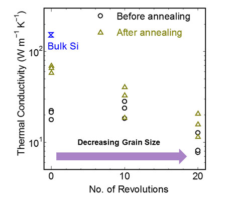
| Reporting their findings in the June 28, 2014 online edition of Nanoscale Research Letters ("Thermal conductivity reduction of crystalline silicon by high-pressure torsion"), the team shows that bulk single crystalline silicon, when subjected to intense plastic strain through high-pressure torsion (HPT) processing, shows a dramatic reduction in room temperature thermal conductivity from its intrinsic single crystal value of 142 W m-1 K-1 to a low thermal conductivity of approximately 7.6 W m-1 K-1. | |
 |
|
| Thermal conductivities of the HPT-processed before and after annealing. An order of magnitude reduction in the thermal conductivity of Si upon HPT processing is observed. Annealing of the HPT samples show an increase in thermal conductivity due to the reverse transformation of metastable phases to Si-I cubic diamond phase. (Image: S. Haris, Kyushu University) | |
| A common method to make nanomaterials in bulk is by ball-milling followed by high temperature spark plasma sintering (SPS). The Kyushu University researchers set out to find a more facile way to make nanograin structures in crystalline silicon – and they did this by using high-pressure torsion (24 GPa). | |
| According to the team, the resulting nanostructured silicon shows a factor 20 reduction in thermal conductivity from its intrinsic single crystalline value. | |
| "Our conductivity results are comparable to nanostructured silicon prepared by ball milling and spark plasma sintering approach reported in the literature," says Harish. "Considering the widely adopted method of ball milling followed by plasma sintering in thermoelectric literature to form bulk samples, the current approach could be a promising alternative for such applications." | |
| This technique is simple, fast and economical – the bulk nanomaterial is prepared at room temperature within few minutes. | |
| The scientists note that, so far, they have not yet been able to establish a clear correlation between the grain size and the reduction in thermal conductivity. | |
| "Current understanding of the mechanism behind such a dramatic thermal conductivity reduction using this method is fairly superficial," says Harish. "We need to perform high resolution transmission electron microscopy measurements to understand the microscopic mechanism in greater detail." | |
| So far, the team has only tested silicon material with this high-pressure torsion approach. nevertheless, the results introduce an efficient and irreversible way to make nanograin boundaries and provide a potential tool for the fabrication of thermoelectric materials with improved performance. | |
 By
Michael
Berger
– Michael is author of three books by the Royal Society of Chemistry:
Nano-Society: Pushing the Boundaries of Technology,
Nanotechnology: The Future is Tiny, and
Nanoengineering: The Skills and Tools Making Technology Invisible
Copyright ©
Nanowerk LLC
By
Michael
Berger
– Michael is author of three books by the Royal Society of Chemistry:
Nano-Society: Pushing the Boundaries of Technology,
Nanotechnology: The Future is Tiny, and
Nanoengineering: The Skills and Tools Making Technology Invisible
Copyright ©
Nanowerk LLC
|
|
|
Become a Spotlight guest author! Join our large and growing group of guest contributors. Have you just published a scientific paper or have other exciting developments to share with the nanotechnology community? Here is how to publish on nanowerk.com. |
|