| Posted: May 16, 2006 | |
New techniques for fabricating carbon nanotube field emission displays |
|
| (Nanowerk Spotlight) A field emission display (FED) is new class of large area, high resolution flat panel display. FEDs use a matrix-addressed cold-cathode to produce light from a cathodoluminescent phosphor screen, just like an array of cathode ray tubes (CRTs). FEDs have many advantageous features: thin panel thickness, self-emissive, distortion free image, wide viewing angle (about 170°), quick response by controlling with analog or digital signals without active elements, tolerance to environment as high as that of receiving tubes, etc. | |
| However, the development of FEDs has not proceeded smoothly due to difficult technological issues such as microfabrication of cathodes and complication of device structure. These isues either caused cost to increase greatly or they limited the display’s fabrication sizes. | |
|
To solve the problem of very high cost for FED fabrication, we developed a set of techniques based on fully printing process. The inner structural layers are prepared by the screen-printing method. The scientific core of these techniques include three innovations:
|
|
  |
|
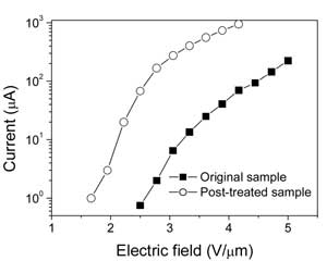
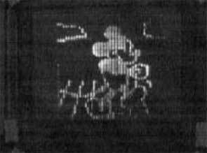
| Left: Field emission curves of printed CNT film before and after treatment. Right: A picture of a moving image displayed by our CNT-FED. (Source: Fan-Guang Zeng, Xi’an Jiaotong University ) | |
| Our techniques provide a route to manufacture a new generation flat panel display devices. Using our techniques, one can make very large CNT field emission displays or display elements under not too high resolution. For example, varied CNT-FEDs manufactured with our techniques can be used in all the cases of using vacuum fluorescent displays (VFDs) or under extreme conditions such as outdoor in very hot or very cold weather. Also, one can use our method to fabricate other information display devices, such as traffic signal lamps, pixel array modules and flat panel display walls. | |
| Our work related to the fabrication of CNT-FED was introduced in the paper titled “The fabrication and operation of fully printed carbon nanotube field emission displays”, published in the June, 2006 issue of Microelectronics Journal. The work on the improvement of luminescent stability/lifetime will be published in Science in China Series E: Technological Sciences 49 (3), 2006. | |
| By Professor Fan-Guang Zeng, Department of Automatic Engineering, Zhengzhou Institute of Aeronautical Industry Management, PR China | |
Become a Spotlight guest author! Join our large and growing group of guest contributors. Have you just published a scientific paper or have other exciting developments to share with the nanotechnology community? Here is how to publish on nanowerk.com.