Showing Spotlights 25 - 32 of 48 in category All (newest first):
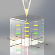
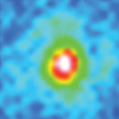 Luminescent quantum dots (LQDs), which possess high photoluminescence quantum yields, flexible emission color controlling, and solution processibility, are promising for applications in lighting systems (warm white light without UV and infrared irradiation) and high quality displays. However, the commercialization of LQDs has been held back by the prohibitively high cost of their production. In a breakthrough approach, researchers have now succeeded in preparing highly emissive inorganic perovskite quantum dots at room temperature.
Mar 7th, 2016
 Compared to the conventional inefficient incandescent and fluorescent lighting technologies, LED light bulbs can, in principle, operate at an efficiency level of 100%. The current LED lighting technology, however, is not even close to reaching this limit. This is due to several problems which, however, can be by and large solved by employing tunnel junction integration into current nanowire LED structures. Demonstrating this, researchers have developed tunnel junction nanowire LEDs that can eliminate the use of resistive p-GaN contact layers, leading to reduced voltage loss and enhanced hole injection.
Oct 15th, 2015
 Polymer Dispersed Liquid Crystals (PDLCs) are micrometer-sized birefringent Liquid Crystal domains dispersed in an optically transparent continuous polymer matrix. The peculiarity of a PDLC system is that of scattering different amounts of an impinging light beam intensity, depending on the strength of an external electric field that is, eventually, applied to the system. A new generation of polymer-dispersed liquid crystals is based on a room temperature, polymerizable, nematic LC host.
Jan 13th, 2015
 White-light-emitting diodes have many advantages over forms of lighting - incandescent, fluorescent and halogen - and this solid-state lighting technique is bound to make major inroads into the commercial and household markets. Researchers have now designed precursors and chemical processes to synthesize intercrossed carbon nanomaterials with relatively pure hydroxy surface states for the first time, which enable them to overcome the aggregation-induced quenching (AIQ) effect, and to emit stable yellow-orange luminescence in both colloidal and solid states.
Nov 25th, 2014
 Researchers have demonstrated that they can print interwoven structures of quantum dots, polymers, metal nanoparticles, etc, to create the first fully 3D printed LEDs, in which every component is 3D printed. At the fundamental level, 3D printing should be entirely capable of creating spatially heterogeneous multi-material structures by dispensing a wide range of material classes with disparate viscosities and functionalities, including semiconducting colloidal nanomaterials, elastomeric matrices, organic polymers, and liquid and solid metals.
Nov 5th, 2014
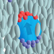 Impurities during the production process of liquid crystal devices result in mobile ions that influence the LCs' field-induced switching phenomena, resulting in a phenomenon called image sticking, or ghosting. Researchers now have developed a method to reduce the presence of excess ions by doping LCDs with ferroelectric nanoparticles. They demonstrate that this reduction of free ions has coherent impacts on the LC's conductivity, rotational viscosity, and electric field-induced nematic switching.
Oct 16th, 2014
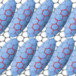 Ferroelectric liquid crystal (FLC) display technology holds the promise of fast switching times, a large viewing angle, and high resolution. FLCs have a spontaneous polarization whose direction is perpendicular to the layer. This spontaneous polarization plays an imperative role in the electro-optic switching of FLCs. Researchers have now developed a technique to amplify the spontaneous polarization by doping graphene into FLCs.
Sep 18th, 2014
 The light-emitting electrochemical cell (LEC) shares several external attributes with the OLED, notably the opportunity for soft areal emission from thin-film devices, but its unique electrochemical operation eliminates the principal requirement on inert-atmosphere/vacuum processing as it can comprise solely air-stabile materials. This important intrinsic advantage has inspired recent work on an ambient-air fabrication of LEC devices using scalable means. Introducing a new, purpose-designed spray-sintering deposition technique, researchers have now shown that it is possible to spray out liquid inks onto essentially any surface for the achievement of light emission.
Jun 2nd, 2014
 Subscribe to our Nanotechnology Spotlight feed