| Posted: Jun 18, 2014 |
Nanoengineering boosts carrier multiplication in quantum dots four-fold
|
|
(Nanowerk News) Los Alamos researchers have demonstrated an almost four-fold boost of the carrier multiplication yield with nanoengineered quantum dots. Carrier multiplication is when a single photon can excite multiple electrons. Quantum dots are novel nanostructures that can become the basis of the next generation of solar cells, capable of squeezing additional electricity out of the extra energy of blue and ultraviolet photons.
|
|
“Typical solar cells absorb a wide portion of the solar spectrum, but because of the rapid cooling of energetic (or ‘hot’) charge carriers, the extra energy of blue and ultraviolet solar photons is wasted in producing heat,” said Victor Klimov, director of the Center for Advanced Solar Photophysics (CASP) at Los Alamos National Laboratory.
|
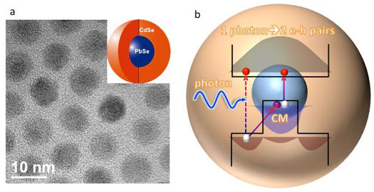 |
| Core/shell PbSe/CdSe quantum dots (a) and a carrier multiplication (CM) pathway (b) in these nano structures. (a) Transmission electron microscopy image of thick-shell PbSe/CdSe quantum dots developed for this study. (b) A hot hole generated in the shell via absorption of a photon collides with a core-localized valence-band electron, promoting it across the energy-gap, which generates a second electron-hole pair. In thick-shell PbSe/CdSe quantum dots this process is enhanced due to slow relaxation of shell-localized holes into the core.
|
|
Getting two for the price of one
|
|
“In principle, this lost energy can be recovered by converting it into additional photocurrent via carrier multiplication. In that case, collision of a hot carrier with a valence-band electron excites it across the energy gap,” Klimov said. “In this way, absorption of a single photon from the high-energy end of the solar spectrum produces not just one but two electron-hole pairs, which in terms of power output means getting two for the price of one.”
|
|
Carrier multiplication is inefficient in the bulk solids used in ordinary solar cells but is appreciably enhanced in ultrasmall semiconductor particles – also called quantum dots -- as was first demonstrated by LANL researchers in 2004 (Schaller & Klimov, Phys. Rev. Lett. 92, 186601, 2004). In conventional quantum dots, however, carrier multiplication is not efficient enough to boost the power output of practical devices.
|
|
A new study ("Enhanced carrier multiplication in engineered quasi-type-II quantum dots") conducted within the Center for Advanced Solar Photophysics demonstrates that appropriately engineered core/shell nanostructures made of lead selenide and cadmium selenide (PbSe and CdSe) can increase the carrier multiplication yield four-fold over simple PbSe quantum dots.
|
|
Klimov explained, “This strong enhancement is derived primarily from the unusually slow phonon relaxation of hot holes that become trapped in high-energy states within the thick CdSe shell. The long lifetime of these energetic holes facilitates an alternative relaxation mechanism via collisions with core-localized valence band electron which leads to highly efficient carrier multiplication.”
|
|
The nuts and bolts of slowing cooling
|
|
To realize the effect of slowed carrier cooling LANL researchers have fabricated PbSe quantum dots with an especially thick CdSe shell. Qianglu Lin, a CASP student working on the synthesis of these materials said, “A striking feature of the thick-shell PbSe/CdSe quantum dots is fairly bright visible emission, from the shell, observed simultaneously with the infrared emission from the core. This shows that intraband cooling is slowed down dramatically, so that holes reside in the shell long enough to produce emission.”
|
|
|
|
“This slowed relaxation, which underlies the observed enhancement of carrier multiplication, likely relates to the interplay between core- versus shell-localization of valence-band states” explained Nikolay Makarov, a spectroscopist working on this project. Istvan Robel, another CASP member added “Our modeling indicates that when the shell is thick enough, the higher-energy hole states lay primarily in the shell, while lower-energy states still remain confined to the core. This separation leads to electronic decoupling of higher- from lower-energy holes states, which is responsible for the observed slowed cooling.”
|
|
What this could mean in future
|
|
While the present CASP work is based on PbSe/CdSe quantum dots, the concept of “carrier-multiplication engineering” through control of intraband cooling is general, and should be realizable with other combinations of materials and/or nanostructure geometries.
|
|
Jeff Pietryga, lead CASP chemist says, “Further enhancement in carrier multiplication should be possible by combining this new approach with other demonstrated means for increasing multicarrier yields, such as by using shape-control (as in nanorods) and/or materials in which cooling is already naturally slower, like PbTe.” Applied together, these strategies might provide a practical route to nanostructures exhibiting carrier multiplication performance approaching the limits imposed by energy conservation.
|

