| Posted: Oct 17, 2014 |
Self-assembly fabricating method for graphene nanoribbons brings scientists a step closer to revolutionizing electronics
|
|
(Nanowerk News) First characterized in 2004, graphene is a two-dimensional material with extraordinary properties. The thickness of just one carbon atom, and hundreds of times faster at conducting heat and charge than silicon, graphene is expected to revolutionize high-speed transistors in the near future.
|
|
Graphene’s exotic electronic and magnetic properties can be tailored by cutting large sheets of the material down to ribbons of specific lengths and edge configurations — scientists have theorized that nanoribbons with zigzag edges are the most magnetic, making them suitable for spintronics applications. (Spintronics devices, unlike conventional electronics, use electrons’ spins rather than their charge.)
|
|
But this “top-down” fabrication approach is not yet practical, because current lithographic techniques for tailoring the ribbons always produce defects.
|
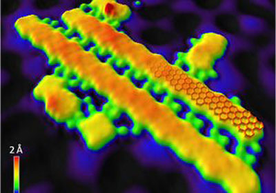 |
| Graphene nanoribbons imaged by scanning tunneling microscopy. The zigzag edges are highlighted by the red structure. (Image: Patrick Han)
|
|
Now, scientists from UCLA and Tohoku University have discovered a new self-assembly method for producing defect-free graphene nanoribbons with periodic zigzag-edge regions. In this “bottom-up” technique, researchers use a copper substrate’s unique properties to change the way the precursor molecules react to one another as they assemble into graphene nanoribbons. This allows the scientists to control the nanoribbons’ length, edge configuration and location on the substrate.
|
|
This new method of graphene fabrication by self-assembly is a stepping stone toward the production of self-assembled graphene devices that will vastly improve the performance of data storage circuits, batteries and electronics.
|
|
Paul Weiss, distinguished professor of chemistry and biochemistry and a member of UCLA’s California NanoSystems Institute, developed the method for producing the nanoribbons with Patrick Han and Taro Hitosugi, professors at the Advanced Institute of Materials Research at Tohoku University in Sendai, Japan, of which Weiss is also a member. The study was published recently in the journal ACS Nano ("Bottom-Up Graphene-Nanoribbon Fabrication Reveals Chiral Edges and Enantioselectivity").
|
|
“To make devices out of graphene, we need to control its geometric and electronic structures,” Weiss said. “Making zigzag edges does both of these simultaneously, as there are some special properties of graphene nanoribbons with zigzag edges. Having these in hand will enable us to test theoretical predictions about them, such as magnetic properties.”
|
|
Other bottom-up methods of fabricating graphene have been attempted, but they have produced bundles of ribbons that need to be subsequently isolated and positioned for use in devices.
|
|
“Previous strategies in bottom-up molecular assemblies used inert substrates, such as gold or silver, to give molecules a lot of freedom to diffuse and react on the surface,” Han said. “But this also means that the way these molecules assemble is completely determined by the intermolecular forces and by the molecular chemistry. Our method opens the possibility for self-assembling single-graphene devices at desired locations, because of the length and the direction control.”
|

