| Posted: Jul 24, 2015 |
Illuminating the electronic properties of graphene
|
|
(Nanowerk News) For the last decade, the usual way of measuring the electronic properties of graphene – in particular the carrier mobility and carrier density, which together give the sheet conductance – has been to fabricate a transistor-like device and electronically measure how the conductance changes as a function of applied electrostatic gate voltage.
|
|
This all-electronic approach is best when dealing with small pieces of graphene, such as the microscopic flakes produced by micromechanical cleavage (also known as the ‘scotch-tape method’) – however, advances in graphene production techniques now allow us to continuously produce large areas of graphene meters across.
|
|
Producing and measuring thousands or millions of microscopic devices from such sheets would be impractical and would reduce the useful area of graphene for the intended application. We need to be able to check the electronic properties of such large regions without destroying them in the process.
|
|
Researchers at the Technical University of Denmark (DTU) have shown that both the carrier mobility and the carrier density of graphene can be measured in a spatially resolved and non-destructive way – providing ‘maps’ of the electronic properties critical for the successful use of graphene in photovoltaics, electronics, spintronics and optics – using terahertz (THz) radiation and doing away with the need to fabricate devices.
|
|
Using a procedure known as THz time-domain spectroscopy, Jonas Buron and colleagues from DTU research teams led by Peter Uhd Jepsen and Peter Bøggild measured the carrier mobility and carrier density at tens of thousands of points in a centimetre sized single layer of graphene (Scientific Reports, "Graphene mobility mapping").
|
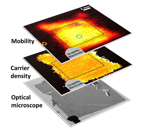 |
| Bottom: Tiled optical ultra-high resolution image of CVD graphene sample on THz-transparent, layered substrate. Middle and top: Maps showing the spatial distribution of carrier density and hole field effect mobility across the CVD graphene film evaluated at 0.5–0.9 THz. (Image: DTU Nanotech) (click on image to enlarge)
|
|
A key enabling step in these first contact-free measurements of the electronic properties of graphene was the realisation that the graphene conductance could be tuned during the measurements using a back-gate, which is transparent to THz radiation.
|
|
"While we still need to transfer the graphene to a special substrate with the THz-invisible gate, it is far easier and less destructive than conventional techniques... and much, much faster", says Jonas Buron. For many electronic applications of graphene, the fabrication of a back-gate is a necessary step anyway. "With some optimisation we could potentially map the carrier mobility and density of a graphene-coated 4-inch wafer in minutes."
|
|
The maps of the electronic properties of graphene are already providing insight and surprises about the origin of their spatial variation – in one sample, the researchers observed twice as much variation in mobility as in carrier density. Variations in conductance are usually ascribed to carrier density changes due to doping variations, but the researchers proved that here this was not the case.
|
|
“We have often noted such slow variations of the conductivity across many centimeters in THz measurements,” Peter Bøggild explained. “But since graphene is so easily doped due to its extreme surface-to-volume ratio, we always expected these to be related to local doping level variations. In this case, we have the exact opposite situation, and this is puzzling. Without this mobility mapping technique we would never have known."
|
|
The THz-TDS technique has a strong potential, adds Peter Uhd Jepsen. "It is already surprising how deep information we can extract from transmitting radiation through a just 0.3 nm thin sheet of carbon atoms, which is supported by a 1.5 million times thicker piece of silicon. We are still learning how to characterise electric properties of graphene without electric contacts, and there are excellent options for improving and speeding up the technique."
|


