| Posted: Dec 03, 2015 |
Researchers make transparent conductors by means of stamping and growing(Nanowerk News) Researchers from FOM Institute AMOLF have discovered a new technique to make transparent conductors used in electronics such as solar cells and smartphones. The technique is a combination of a stamping mechanism on the nanoscale and a chemical process. Compared with existing production methods, this new technique results in a better conducting product at lower costs. The researchers will publish the results online on 3 December in the journal Advanced Materials ("Solution-grown Silver Nanowire Ordered Arrays as Transparent Electrodes"). |
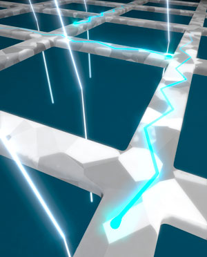 |
| The image shows a network of silver nanowires created with the new technique. The white lines running from top to bottom represent rays of light, which move in a straight line through the lattice. The blue lines are the electrons that cannot pass straight through, because they are scattered at the boundaries between the silver crystals. Individual crystals are visible via the colour contrast. |
| Stamping followed by a chemical process in water |
| The researchers based the new process on a combination of two existing techniques. Using the stamping technique 'Substrate Conformal Imprint Lithography', which originates from a collaboration between Philips and AMOLF, they stamped a pattern in a thin layer of plastic on top of a glass substrate. The result looks much like a nanoscale landscape: a surface that is crisscrossed with interconnecting channels. The researchers subsequently filled the minuscule channels with silver using a chemical process known as the 'Tollens' reaction'. After removing the plastic, a conductive silver grid remains on the glass substrate. The patterns of this conductor are smaller than the wavelength of light; as a result, they do not reflect any colours from the visible spectrum. This property makes the conductor transparent. |
| Advantages |
| The new technique offers several advantages. The network consists of silver crystals that are neatly arranged and nearly as wide as the stamped channels. This means there are relatively few boundaries between the crystals, which facilitates electron flow through the network. Consequently, the technique has a conductivity three times as high as a conventional method based on the evaporation of metals. For that evaporation method, researchers use the same plastic nanopattern but the metal deposits everywhere, not only in the channels. This means that when the plastic is peeled off, some of the metal is wasted. Additionally, the evaporation requires a lot of energy. |
| AMOLF postdoc Beniamino Sciacca: "We combine the best of both worlds. The structures with nanopatterns have proved their value and remain part of the process, but the application of the metal layer on the structure yields better results in the solution. We lose less metal and it is more energy efficient." Project leader Erik Garnett: "In view of the many advantages, I think there is a good chance the technique will find its way to commercial applications such as solar cells, tablets and smartphones." |
| Source: FOM |

