| Posted: Jul 26, 2017 |
Compact Brillouin devices through hybrid integration on silicon
(Nanowerk News) Integrated circuits, so called chips, are used in everyday electronic equipment like mobile phones and computers. It is a set of electronic circuits on one small flat piece of semiconductor material, normally silicon. But this material has some limitations when it comes to processing data.
|
|
To overcome these limitations and improve data processing, researchers are developing optical circuits made of chalcogenide glass. This special type of glass is used for ultrafast telecommunication networks, transferring information at the speed of light.
|
|
Integrating these glass optical circuits into silicon chips could lead to a more advanced communications system, processing data a hundred times faster. Can these two materials be combined?
|
|
The answer is yes! In a collaboration with physicists in the University of Sydney's Australian Institute for Nanoscale Science and Technology (AINST), the Australian National University (ANU) and RMIT University, the CUDOS research group around PhD candidate Blair Morrison and senior researcher Dr Alvaro Casas Bedoya created compact, mass manufacturable optical circuits with enhanced functionalities by combining nonlinear glasses with silicon-based material.
|
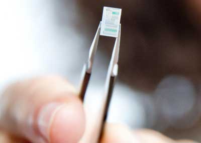 |
| The new device is smaller than a thumbnail with a size of 0.1 x 4mm, and could be integrated into everyday electronic devices like smartphones. (Image: CUDOS)
|
|
"In the last few years the group at the University of Sydney has repeatedly demonstrated exciting functionalities, such as broadband microwave devices that enhance radar and countermeasure technologies, using these novel chalcogenide glasses," Blair Morrison said from the University of Sydney CUDOS node.
|
|
"Now we have shown it is possible to combine this material with the current industry standard platform for photonic integration, silicon," he said.
|
|
"We integrated a novel nonlinear glass into an industrially scalable CMOS compatible platform. We maintained the key advantages of both the silicon and the glass, and made a functional and efficient ultra-compact optical circuit," said Dr Alvaro Casas Bedoya who is the lead photonics nanofabrication manager for CUDOS.
|
|
"A wealth of new opportunities will be created, and this takes us one step closer to moving our research from the lab into industrial applications," said Blair Morrison.
|
|
CUDOS Director and ARC Laureate Fellow Professor Benjamin Eggleton from the University of Sydney said this new approach will one day allow the industry to miniaturise the photonics functionalities from devices that are the size of a laptop to the size of a smartphone and even smaller, allowing for deployment in real world applications.
|
|
"This is exciting, because this is a platform which is more compatible with existing semiconductor manufacturing and will allow us to integrate multiple functionalities on a single silicon chip, with active and passive components, such as detectors and modulators, required for advanced applications," said Professor Eggleton who supervised the project.
|
|
The multi-university research team went through the whole manufacturing process: The fabrication of these devices uses silicon wafers from a semiconductor foundry in Belgium, a dedicated facility in ANU's Laser Physics Centre for the glass deposition, lithography in the RMIT University's School of Engineering and are then characterised and tested in the University of Sydney's AINST.
|
|
To showcase the potential of the new approach, the CUDOS researchers further demonstrated a compact novel laser based on the light-sound interactions, the first time in an integrated optical circuit.
|
|
"The breakthrough here is this realisation that we can actually interface, we can integrate that glass onto silicon and we can interface from silicon to the glass very efficiently - we can harness the best of both worlds," Professor Eggleton said.
|
|
The research is published in Optica ("Compact Brillouin devices through hybrid integration on silicon").
|
|
Professor Susan Pond, the Director of AINST, emphasized that this project is one of AINST flagship activities that deals with harnessing interactions between photons and phonon at the nanoscale. This work links fundamental research in light matter interactions at the nanoscale with an end user perspective and strong coupling to industry.
|

