| Posted: Oct 19, 2017 |
Extreme light trapping with nanomaterials
(Nanowerk News) A silicon solar cell harvests the energy of the sun as light travels down through light-absorbent silicon. To reduce weight and cost, solar cells are thin, and while silicon absorbs visible light well, it captures less than half of the light in the near-infrared spectrum, which makes up one-third of the sun’s energy. The depth of the material limits absorption. But what if light within the cell could be channeled horizontally so that silicon could absorb its energy along the width of the cell rather than its depth?
|
|
With such an advance in mind, Shawn-Yu Lin, professor of physics, applied physics, and astronomy at Rensselaer Polytechnic Institute, has built a nanostructure whose crystal lattice bends light as it enters the material and directs it in a path parallel to the surface, known as “parallel to interface refraction.” The structure is built of overlapping nanotubes and resembles a three-dimensional grid made of Lincoln Logs. Photonic nanocrystals built using his process enable extreme “light trapping” and could have applications from thin-film solar cells to photo-chemical functions like sensing and water splitting.
|
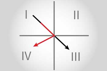 |
| Light from quadrant I usually refracts within quadrant III. But in parallel to interface refraction, the light is bent into quadrant IV. (Image: Rensselaer Polytechnic Institute)
|
|
“These results prove that this effect exists, that if you follow my guidelines of simple cubic symmetry, you can bend light by 90 degrees. The photonic crystal forces light to bend in a deterministic manner, rather than random scattering or surface effects,” said Lin. “This is a new type of light-matter interaction that lies at the heart of what light trapping is intended to do.”
|
|
In experimental results, which appear in Nature Scientific Reports ("Effectively infinite optical path-length created using a simple cubic photonic crystal for extreme light trapping"), Lin created a photonic crystal using titanium dioxide, a material with weak visible light absorption, to prove the success of the effect. Results using a 900-nanometer thick titanium dioxide photonic nanocrystal showed absorption enhanced by one to two orders of magnitude greater than a reference film of the same material for some regions. Lin built the nanocrystal – first in silicon, now in titanium dioxide – based on the theoretical predictions of his collaborator, Sajeev John, a physicist at the University of Toronto.
|
|
Light trapping describes the process of confining light to a given space, usually with the intent of converting it to other forms of energy. In one approach, materials are designed to slow light, so that it spends more time in the material. In the approach Lin used, the light is bent away from its given path, making it travel a longer distance within the material, in this case, the full width of a titanium dioxide wafer.
|
|
Light always bends somewhat as it enters a material with a different optical index, something easily seen as light enters water. In water, and many other materials, the light bends only slightly. The arrangement of atoms in the titanium dioxide crystal Lin created matches the scale of visible light wavelengths, scattering light at multiple points in space simultaneously as it moves into the lattice. As a consequence, light cannot move as it does through space or any continuous medium. Instead, it is bent at an obtuse angle – a phenomenon known as “negative refraction” – and channeled along the width of the material.
|
|
To manipulate the flow of visible light, with wavelengths ranging from 400 to 700 nanometers, Lin pioneered a method of building a perfectly symmetrical cube of nanotubes to match the scale of the light. First, a layer of titanium dioxide is deposited on a substrate. Then, a thin layer of chromium dioxide is deposited to serve as a mask for a photolithographic process that etches lines into the titanium dioxide. Once completed, a solvent is used to remove the remaining chromium dioxide, completing the first layer of “logs.” To build additional layers, a layer of silicon dioxide is deposited to fill the cavities between the logs, the surface is polished flat to the top of the first layer, and the entire process is repeated at a precise 90-degree angle from the first layer.
|
|
One layer of the material is less than 1 millionth of a meter – or micron – thick, but was produced in wafers 100 millimeters wide, giving the material as much as 100,000 times the space to absorb light.
|
|
“This discovery proves a huge enhancement in path length when using a material that has a very low absorption. Its discovery changes the name of the game from vertically absorbed, to horizontally absorbed in a super thin structure,” said Lin.
|

