| May 30, 2019 |
Quantum information gets a boost from thin-film breakthrough(Nanowerk News) Efforts to create reliable light-based quantum computing, quantum key distribution for cybersecurity, and other technologies got a boost from a new study demonstrating an innovative method for creating thin films to control the emission of single photons. |
| “Efficiently controlling certain thin-film materials so they emit single photons at precise locations—what’s known as deterministic quantum emission—paves the way for beyond-lab-scale quantum materials,” said Michael Pettes, a Los Alamos National Laboratory materials scientist and leader of the multi-institution research team. |
| The scalability of these two-dimensional, tungsten/selenium thin films makes them potentially useful in processes to manufacture quantum technologies. Single-photon generation is a requirement for all-optical quantum computing and key distribution in quantum communications, and it is crucial for advancing quantum information technologies. |
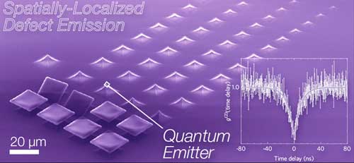 |
| An innovative method for controlling single-photon emission for specific locations in 2D materials may offer a new path toward all-optical quantum computers and other quantum technologies. This image shows a false-color scanning electron micrograph of the array used to create place single-photon sources in epitaxial tungsten diselenide. Inset shows the Hanbury-Brown Twiss interferometry measurement proving quantum emission. (Image: LANL) |
| The project, documented as a Featured Article in the journal Applied Physics Letters ("Locally Defined Quantum Emission from Epitaxial Few-Layer Tungsten Diselenide"), exploits strain at highly spatially localized and well-separated emission sites, or tips, in a tungsten/selenium film. The team synthesized the film through chemical vapor deposition using a multi-step, diffusion-mediated gas source. |
| Because the material is very thin, it conforms to the radius of the tips and the material bends towards the substrate by more than a few percent, like someone lying on a bed of nails. The resulting strain is enough to change the electronic structure, but only at the tips. The affected area emits light of a different color and nature than light from the rest of the film. |
| “While more research is needed to fully understand the role of mechanical deformation in creating these quantum emission sites, we may enable a route to control quantum optical properties by using strain,” Pettes said. “These single-photon sources form the basis for photonics-based, all-optical quantum computing schemes.” |
| Engineering of quantum emission in 2D materials is still in a very early stage, the authors note. While studies have observed single photons originating from defect structures in these materials, previous work has suggested that non-uniform strain fields might govern the effect. However, the mechanism responsible for this emergent phenomenon remains unclear and is the focus of ongoing work at Los Alamos. |
| Source: Los Alamos National Laboratory |
|
Subscribe to a free copy of one of our daily Nanowerk Newsletter Email Digests with a compilation of all of the day's news. |

