| Jul 29, 2019 |
Transfer-printing technology for creating flexible sensors on topographic surfaces(Nanowerk News) The Korea Institute of Science and Technology (KIST, president: Byung-gwon Lee) announced that Dr. Hyunjung Yi of the Post-Silicon Semiconductor Institute and her research team developed a transfer-printing technology (a process for producing electrical devices via which electrodes are printed on a transfer mold and then transferred to a final substrate) that uses hydrogel and nano ink to easily create high-performance sensors on flexible substrates of diverse shapes and structures (Nano Letters, "Hydrogel-Templated Transfer-Printing of Conductive Nanonetworks for Wearable Sensors on Topographic Flexible Substrates"). |
| Interest in wearable devices, including smartwatches and fitness bands, is increasing rapidly. With the scope of such devices expanding from types that are worn (like clothing) to those that are attached directly to the skin, there is growing demand for technologies that allow for the production of high-performance sensors on surfaces of various shapes and types. |
| Transfer printing works in a way similar to that of a tattoo sticker: just as sticking the tattoo sticker onto the skin and then removing the paper section leaves the image on the skin, this process creates a structure on one surface and then transfers it onto another. |
| The most notable advantage of this process is that it largely avoids the difficulties involved in creating devices directly on substrates that are thermally and/or chemically sensitive, which is why transfer printing is widely used for the manufacturing of flexible devices. On the other hand, the primary disadvantage of current transfer printing processes is that they can usually only be used for substrates with flat surfaces. |
| The KIST team overcame these limitations by developing a simple and easy transfer printing process that allows for the creation of high-performance, flexible sensors on topographic surfaces with diverse features and textures. |
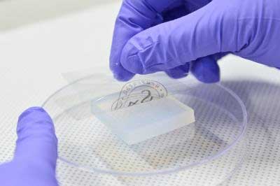 |
| It is easily transferring electrodes on top of hydrogel (bottom) to PET film (top) with the transfer-printing technology that was developed by a researcher of KIST's Post-Silicon Semiconductor. (Image: KIST) |
| Using the porous and hydrophilic nature of hydrogels, the KIST team inkjet-printed an aqueous solution-based nano ink onto a hydrogel layer (which was solidified onto a topographic surface). The surfactant and water in the nano ink passed quickly through the hydrogel's porous structure, leaving only the hydrophobic nanomaterial (the particles of which are greater in length than the diameter of the holes in the hydrogel) remaining on the surface, allowing for the creation of the desired electrode pattern. |
| The amount of nano ink used for this printing process was very small, allowing for the rapid formation of electrodes. Moreover, the electrical performance of the electrodes was outstanding, due to the high levels of purity and uniformity of the resulting nanonetworks. Also, because of the hydrophobic nature of the nanomaterial, there was an extremely low degree of interaction between it and the hydrogel, allowing for the easy transfer of the electrodes to diverse topographic surfaces. |
| In particular, the KIST team developed a technology for transferring nanonetworks by employing a method that solidifies a moldable elastomeric fluid onto a hydrogel surface, enabling the easy creation of flexible electrodes even on substrates with rough surfaces. The team transferred nanoelectrodes directly onto a glove to create a modified sensor that can immediately detect finger movements. It also created a flexible, high-performance pressure sensor that can measure the pulse in the wrist. |
| Yi said, "The outcome of this study is a new and easy method for creating flexible, high-performance sensors on surfaces with diverse characteristics and structures. We expect that this study will be utilized in the many areas that require the application of high-performance materials onto flexible and/or non-traditional substrates, including digital healthcare, intelligent human-machine interfaces, medical engineering, and next-generation electrical materials." |
| Source: Korea Institute of Science and Technology |
|
Subscribe to a free copy of one of our daily Nanowerk Newsletter Email Digests with a compilation of all of the day's news. |

