| Sep 04, 2019 |
'Resonance' Raman spectroscopy with 1-nm resolution(Nanowerk News) Tip-enhanced Raman spectroscopy resolved “resonance” Raman scattering with 1-nm resolution in ultrathin zinc oxide films epitaxially grown on a single-crystal silver surface (Nano Letters, "Resolving the Correlation between Tip-Enhanced Resonance Raman Scattering and Local Electronic States with 1 nm Resolution"). |
| Tip-enhanced “resonance” Raman scattering can be used to investigate a specific chemical structure at nanoscale and even at the single-molecule level and also provides a new approach for the atomic-scale optical characterization of local electronic states. |
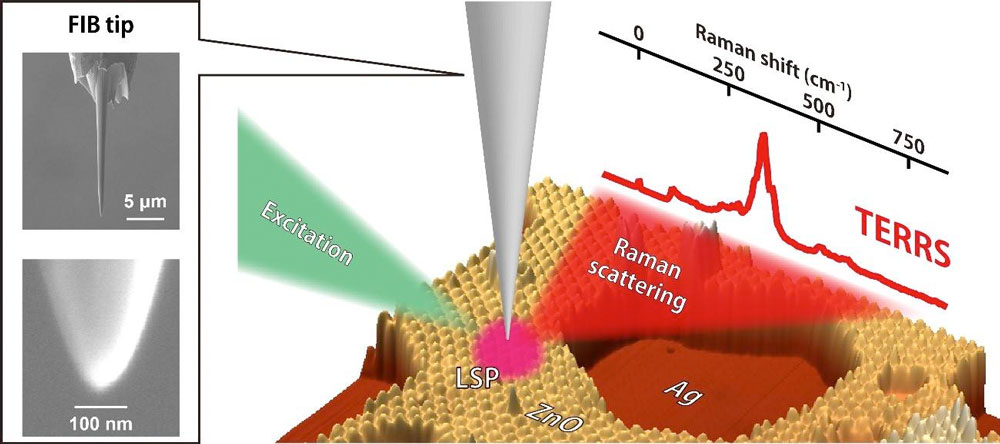 |
| Fig. 1 Schematic of tip-enhanced resonance Raman scattering measurement. Tip-enhanced resonance Raman scattering is measured by a silver tip fabricated by focused ion beam (FIB) milling. Localized surface plasmon (LSP) is excited by an excitation laser, which generates enhanced Raman scattering from ultrathin zinc oxide (ZnO) films grown on a single-crystal silver (Ag) surface. (Image: Takashi Kumagai) (click on image to enlarge) |
| This will be a powerful tool to study, for instance, local defects in low-dimensional materials and active sites of heterogeneous catalysis. |
| A research team at Fritz-Haber Institute in Berlin, headed by Dr. Takashi Kumagai, demonstrated tip-enhanced “resonance” Raman spectroscopy. Resonance Raman spectroscopy is a powerful tool to analyze a specific chemical structure at a high sensitivity, but its spatial resolution has been restricted to be a few hundred nm due to the diffraction limit. |
| Extreme field confinement at a metal tip apex through localized surface plasmon excitation allows to break this limitation and now attain 1-nm resolution. Tip-enhanced Raman spectroscopy takes advantage of atomic resolution imaging of scanning probe microscopy and enhanced Raman scattering through localized surface plasmon excitation. |
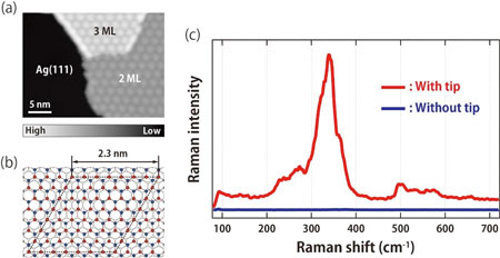 |
| Fig.2 Tip-enhanced resonance Raman spectrum of ultrathin ZnO films on a Ag(111) surface. (a) STM image of 2- and 3-monolayer ZnO films epitaxially grown on Ag(111) at 78 K. (b) Schematic of the ZnO film. (c) Tip-enhanced resonance Raman spectrum of the ZnO film. (Image: Takashi Kumagai) |
| The research team revealed tip-enhanced resonance Raman scattering in which both physical and chemical enhancement mechanisms are operative. The underlying process was examined by modifying the localized surface plasmon resonance in the scanning tunneling microscope junction and by recording different-thickness zinc oxide films that exhibit a slightly different electronic structure. |
| In addition, the correlation between tip-enhanced resonance Raman scattering and local electronic states is resolved in combination with scanning tunneling spectroscopy that maps the local electronic state of the zinc oxide film. |
| These results explicitly show that a confined electromagnetic field can interact with local electronic resonances at the (sub)nanometer scale. |
| Source: Japan Science and Technology Agency |
|
Subscribe to a free copy of one of our daily Nanowerk Newsletter Email Digests with a compilation of all of the day's news. |

