| Nov 19, 2019 |
Clean carbon nanotubes with superb properties(Nanowerk News) Single-wall carbon nanotubes (SWCNT) have found many uses in electronics and new touch screen devices. Carbon nanotubes are sheets of one atom-thick layer of graphene rolled up seamlessly into different sizes and shapes. To be able to use them in commercial products like transparent transistors for phone screens, researchers need to be able to easily test nanotubes for their materials properties, and the new method helps with this. |
| Professor Esko I. Kauppinen's group at Aalto has years of experience in making carbon nanotubes for electronic applications. The team's unique method uses aerosols of metal catalysts and gasses containing carbon. This aerosol-based method allows the researchers to carefully control the nanotube structure directly. |
| Fabricating single carbon nanotube transistors is usually tedious. It often takes days from raw carbon nanotube material to transistors, and the devices were contaminated with processing chemicals, degrading their performance. |
| However the new method makes it possible to fabricate hundreds of individual carbon nanotube devices within 3 hours, an over ten times increase in efficiency. |
| Most importantly, these fabricated devices do not contain degrading processing chemicals on their surface. These so-called ultra-clean devices have been previously even more difficult to manufacture than regular single carbon nanotube transistors. |
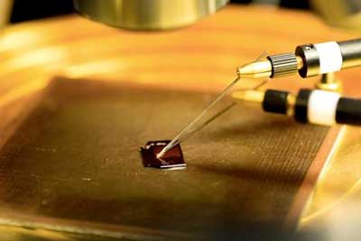 |
| 1000 single nanotube transistors on a chip. (Image: Aalto University) |
| 'These clean devices help us to measure the intrinsic material properties. And the large number of devices helps to get a more systematic understanding of the nanomaterials, rather than just a few data points.' says Dr. Nan Wei, a postdoctoral researcher in the group. |
| This study (Advanced Functional Materials, "Fast and Ultraclean Approach for Measuring the Transport Properties of Carbon Nanotubes") shows the aerosol-based nanotubes are superb in terms of their electronic quality, their ability to conduct electricity is almost as good as theoretically possible for SWCNTs. |
| More importantly, the new method can also contribute to applied research. One example is that by studying the conducting property of SWCNT bundle transistors, scientists may find ways to improve performance of flexible conductive films. This could prove useful for designers trying to build flexible, smash-proof phones. Follow-up work by the groups in Japan and Finland is already underway. |
| Source: Aalto University |
|
Subscribe to a free copy of one of our daily Nanowerk Newsletter Email Digests with a compilation of all of the day's news. |

