| Mar 10, 2020 |
Inverse design software automates design process for optical, nanophotonic structures(Nanowerk News) Stanford University researchers created an inverse design codebase called SPINS that can help researchers explore different design methodologies to find fabricable optical and nanophotonic structures. |
| In the journal Applied Physics Reviews ("Nanophotonic inverse design with SPINS: Software architecture and practical considerations"), Logan Su and colleagues review inverse design’s potential for optical and nanophotonic structures, as well as present and explain how to use their own inverse design codebase. |
| “The idea of inverse design is to use more sophisticated optimization algorithms and automate the search for a structure,” Su explained. “The ultimate goal is to have a designer input their desired performance metrics and simply wait for the algorithm to generate the best possible device.” |
| Integrated photonics has many potential applications, ranging from optical interconnects to sensing to quantum computing. |
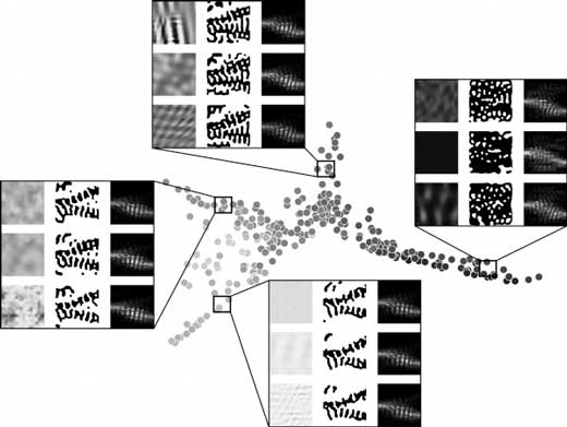 |
| Photonic inverse design produces an assortment of nonintuitive designs that can achieve better performance in smaller footprints than their traditionally designed counterparts can. Despite the multitude of possible designs for any particular task, analysis of the designs for a beam splitter reveals how the algorithm produces devices that can actually be classified into different types based on their structure and underlying physical principles. (Image: Logan Su) |
| Inspired by popular machine learning libraries such as TensorFlow and PyTorch, SPINS is a photonic design framework that emphasizes flexibility and reproducible results. SPINS has been used internally by the group to design an assortment of devices, and the group is making it available for other researchers to use. |
| “The mathematics behind our optimization techniques come from the mathematical optimization community,” Su said. “But we also borrow ideas from the optimization community in mechanical and fluid mechanics, where they use similar optimization methods to design mechanical structures and airfoils before their adoption in photonics.” |
| Inverse design “automates the design process for optical and photonic elements,” he said. “Traditionally, photonic devices are hand designed, in the sense that a designer first comes up with the basic geometric shape of the structures, such as a circle, and then performs a few parameter sweeps of the radius of the circle to improve device performance.” |
| This process is labor intensive and tends to ignore a large class of devices with more complicated shapes that have the potential for much better performance. |
| “Replacing electrical interconnects with photonic interconnects within data centers, for example, could enable an increase in memory bandwidth while substantially decreasing energy costs,” Su said. |
| Photonic neural networks also promise faster operation speeds with lower energy requirements compared to electronic hardware, and metasurface optics promise novel optical functionalities that are cheaper and orders of magnitude smaller than their traditional bulky optical elements. |
| “Part of the barrier to the adoption of these technologies is the performance of the photonic components that comprise that system,” Su said. “By developing a better optimization method for designing these photonic components, we hope to not only improve the performance of these technologies to the point of commercial viability but also open up new possibilities for integrated photonics.” |
| Source: Duke University |
|
Subscribe to a free copy of one of our daily Nanowerk Newsletter Email Digests with a compilation of all of the day's news. |

