| May 28, 2020 |
Nanopatterning electronic properties of twisted 2D semiconductors(Nanowerk News) A team of researchers at the National Graphene Institute, have demonstrated that atomic lattices of slightly twisted 2D transition metal dichalcogenides undergo extensive lattice reconstruction, which can pattern their optoelectronic properties on nanometre length scale. |
| Since the isolation of graphene in 2004, researchers have identified a multitude of 2D materials, each with specific and often exciting properties. |
| More importantly, these atomically thin crystals can be stacked together, similarly to stacking Lego bricks, in order to create artificial materials with desired properties, known as heterostructures. |
| The mutual rotation of adjacent crystals in such heterostructures, or twist, plays an important role in their resulting properties, but so far these studies have largely been limited to graphene and hexagonal boron nitride. |
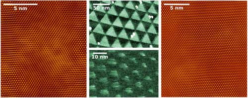 |
| Twisted bilayers of transition metal dichalcogenides. |
| In the report, published in Nature Nanotechnology ("Atomic reconstruction in twisted bilayers of transition metal dichalcogenides"), the team have described that for small twist angles atomic lattices of transition metal dichalcogenides adjust locally to form perfectly stacked bilayer islands, separated by grain boundaries which accumulates the resulting strain. |
| Using atomic resolution transmission electron microscopy (TEM) they have demonstrated that stacking the two monolayers nearly parallel to each other (twist angle close to 0°) and anti-parallel (twist angle close to 180°) produces strikingly different periodic domain patterns. |
| The electronic properties of 2D materials are expected to depend on the local atomic stacking configuration and such periodic domain networks can open an avenue to pattern material properties with nanometre precision. To that end, the team have found that domain in nearly-parallel bilayers demonstrate intrinsic asymmetry of electronic wavefunctions previously unseen in other 2D materials. |
| In anti-parallel bilayers, the resulting domain structure produces strong piezoelectric textures detected by conductive atomic force microscope, which will govern motion of electrons, holes an excitons in this system. |
| This work demonstrates that the “twist” degree of freedom in heterostructure design can allow the creation of new exciting quantum systems, such as controllable periodic arrays of quantum dots and single photon emitters. |
| Astrid Weston, who authored the paper said: “A fundamental understanding of the evolution of crystal structure in twisted transition metal dichalcogenides is critical to the study of their exciting electronic and optical properties and was missing in the field.” |
| Dr Roman Gorbachev, who led the team said: “The twist will have ground-breaking impact on the field of 2D materials, and our work is an important milestone on this path.” |
| Source: University of Manchester |
|
Subscribe to a free copy of one of our daily Nanowerk Newsletter Email Digests with a compilation of all of the day's news. |

