| Jun 12, 2020 |
Two-in-one super molecule for high-density computing(Nanowerk News) NUS Chemists have developed a new type of molecular computing device that acts both as a switch and storage element for nanoelectronic applications (Nature Materials, "Electric Field Driven Dual-Functional Molecular Switches in Tunnel Junctions"). |
| A challenge in miniaturised electronics is to reduce the power consumption, as they cause overheating and reduce battery lifetime in electronic devices. Resistive random access memory (RAM) is generally built by connecting a diode switch in series with a memory element, called “one diode–one resistor”. |
| This approach, however, consumes large amounts of power because the voltage flows across both the diode and the resistor, and the need for the two components makes it more difficult to shrink the size of the devices. |
| By combining both diode and memory within one circuit component, both power consumption and device size can be reduced dramatically, opening the door to ultra-high density computing. |
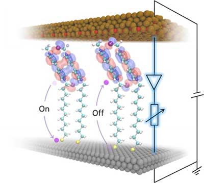 |
| The figure shows the molecular junction with diode+memory dual-function induced by reversible dimerisation of the methyl-viologen headgroups stabilised by directional ion-migration as indicated by the arrows. (Image: NUS) |
| A research team led by Prof Christian NIJHUIS, Department of Chemistry, NUS has developed a new type of molecular switch that works as both a diode and a memory element. This research work is in collaboration with Prof Damien THOMPSON from the University of Limerick, Ireland and Prof Enrique DEL BARCO from the University of Central Florida, USA. |
| The molecular device which they developed is very thin, at only 2 nm thick (length of the molecule) and works with a low drive voltage of less than 1 V. This discovery of being able to perform multiple functionalities within a single molecule may help accelerate the development of new technologies involving artificial synapses and neural networks. |
| Molecular switches are attractive components for computing as they can be designed and tailored to perform specific tasks at extremely small length-scales. Until now, molecular switches in electrical circuits were limited to just a single function and suffered from leakage currents, large variance and short lifetime. The challenge is to stabilise both the on and off states of the switching molecules under the extremely high gigavolt-per-meter electric fields inside the circuits. |
| The molecular switch which the team developed operates in a two-step mechanism, where the injected charge (to store information) is stabilised by the movement of charged ions between the molecules and the surface of the device. This is made possible by pairwise bonding of the molecules. |
| Using a combination of electrical measurements and atomic-scale measurements guided by quantum mechanics, the researchers found an optimal setting to achieve both stability and switchability that allowed it to be used for the dual diode+memory resistive RAM element with a thickness of just 2 nm. Owing to this new charge stabilisation mechanism which also enables fast switching, information can be written into these molecular devices at high speeds for long periods of time with very low power consumption. |
| Prof Nijhuis said, “There are still many challenges that need to be addressed. As we learn more about the mechanism of the dynamic ion migration and changes in potential drops along the molecules in more detail, this will lead us closer towards the aim of designing next-generation computing elements “to order” for specific technology applications.” |
| Source: National University of Singapore |
|
Subscribe to a free copy of one of our daily Nanowerk Newsletter Email Digests with a compilation of all of the day's news. |

