| Aug 13, 2020 |
Coffee stains inspire optimal printing technique for electronics(Nanowerk News) Have you ever spilled your coffee on your desk? You may then have observed one of the most puzzling phenomena of fluid mechanics – the coffee ring effect. This effect has hindered the industrial deployment of functional inks with graphene, 2D materials, and nanoparticles because it makes printed electronic devices behave irregularly. |
| Now, after studying this process for years, a team of researchers have created a new family of inks that overcomes this problem, enabling the fabrication of new electronics such as sensors, light detectors, batteries and solar cells. |
| Coffee rings form because the liquid evaporates quicker at the edges, causing an accumulation of solid particles that results in the characteristic dark ring. Inks behave like coffee – particles in the ink accumulate around the edges creating irregular shapes and uneven surfaces, especially when printing on hard surfaces like silicon wafers or plastics. |
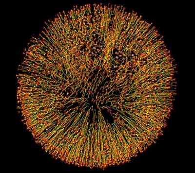 |
| Drying droplets: the red arrows showing the end of the particle trajetories. (Image: Tawfique Hasan) |
| Researchers, led by Tawfique Hasan from the Cambridge Graphene Centre of the University of Cambridge, with Colin Bain from the Department of Chemistry of Durham University, and Meng Zhang from School of Electronic and Information Engineering of Beihang University, studied the physics of ink droplets combining particle tracking in high-speed micro-photography, fluid mechanics, and different combinations of solvents. |
| Their solution: alcohol, specifically a mixture of isopropyl alcohol and 2-butanol. Using these, ink particles tend to distribute evenly across the droplet, generating shapes with uniform thickness and properties. |
| Their results are reported in the journal Science Advances ("A general ink formulation of 2D crystals for wafer-scale inkjet printing"). |
| “The natural form of ink droplets is spherical – however, because of their composition, our ink droplets adopt pancake shapes,” said Hasan. |
| While drying, the new ink droplets deform smoothly across the surface, spreading particles consistently. Using this universal formulation, manufacturers could adopt inkjet printing as a cheap, easy-to-access strategy for the fabrication of electronic devices and sensors. The new inks also avoid the use of polymers or surfactants – commercial additives used to tackle the coffee ring effect, but at the same time thwart the electronic properties of graphene and other 2D materials. |
| Most importantly, the new methodology enables reproducibility and scalability – researchers managed to print 4500 nearly identical devices on a silicon wafer and plastic substrate. In particular, they printed gas sensors and photodetectors, both displaying very little variations in performance. Previously, printing a few hundred such devices was considered a success, even if they showed uneven behaviour. |
| “Understanding this fundamental behaviour of ink droplets has allowed us to find this ideal solution for inkjet printing all kinds of two-dimensional crystals,” said first author Guohua Hu. “Our formulation can be easily scaled up to print new electronic devices on silicon wafers, or plastics, and even in spray painting and wearables, already matching or exceeding the manufacturability requirements for printed devices.” |
| Beyond graphene, the team has optimised over a dozen ink formulations containing different materials. Some of them are graphene two-dimensional ‘cousins’ such as black phosphorus and boron nitride, others are more complex structures like heterostructures – ‘sandwiches’ of different 2D materials – and nanostructured materials. Researchers say their ink formulations can also print pure nanoparticles and organic molecules.This variety of materials could boost the manufacturing of electronic and photonic devices, as well as more efficient catalysts, solar cells, batteries and functional coatings. |
| The team expects to see industrial applications of this technology very soon. Their first proofs of concept – printed sensors and photodetectors – have shown promising results in terms of sensitivity and consistency, exceeding the usual industry requirements. This should attract investors interested in printed and flexible electronics. |
| “Our technology could speed up the adoption of inexpensive, low-power, ultra-connected sensors for the internet of things,” said Hasan. “The dream of smart cities will come true.” |
| Source: University of Cambridge |
|
Subscribe to a free copy of one of our daily Nanowerk Newsletter Email Digests with a compilation of all of the day's news. |

