| Feb 02, 2021 |
Scientists map non-visible materials at nanoscale with ultrasound
(Nanowerk News) The increasing miniaturisation of electrical components in industry requires a new imaging technique at the nanometre scale. Delft researcher Gerard Verbiest and ASML have developed a first proof-of-concept method that they now plan to further develop. The method uses the same principle as ultrasound scanning in pregnancies, but on a much, much smaller scale.
|
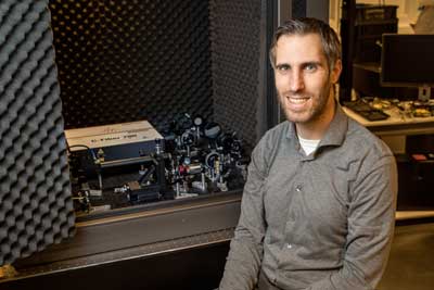 |
| Gerard Verbiest
|
Ultrasound
|
|
‘Existing non-destructive imaging techniques for nanoelectronics, such as optical and electron microscopy, are not accurate enough or applicable to deeper structures,’ explains Gerard Verbiest from Delft's 3mE faculty. ‘A well-known 3D technique on a macro-scale is ultrasound. The advantage here is that it works for every sample. That makes ultrasound an excellent way of mapping the 3D structure of a non-transparent sample in a non-destructive way.’
|
|
And yet, ultrasound technology at the nanoscale didn’t exist yet. Indeed, the resolution of ultrasound imaging is strongly determined by the wavelength of the sound used, and that is typically around a millimetre.
|
AFM
|
|
‘To improve this, ultrasound has already been integrated into an Atomic Force Microscope (AFM),’ Verbiest continues. ‘AFM is a technique that allows you to scan and map out surfaces extremely accurately with a tiny needle. The advantage here is that it isn’t the wavelength but the size of the tip of the AFM that determines the resolution. Unfortunately, at the frequencies used so far (1-10 MHz), the response of the AFM is small and unclear. We do see something, but it’s not clear exactly what we’re seeing. So the frequency of the sound used needed to be further increased, to the GHz range, and that’s what we’ve done.’
|
|
Increasing the frequency is something that has only become possible recently, Verbiest explains. ‘We’re achieving this through photoacoustics. Using the photoacoustic effect allows you to generate extremely short sound pulses. We’ve managed to integrate this technique into an AFM. With the tip of the AFM, we can focus the signal. Our set-up is ready, and we’ve carried out the first tests.’
|
Cell biology
|
|
As mentioned, the new method is particularly interesting for nanoelectronics. ‘If you want to make even smaller chips with even smaller patterns in the future, then this is the step you have to take,’ says Verbiest. ‘For example, to make it possible to place two layers on top of each other with nanometre precision.’
|
|
‘But there are certainly potential applications outside of electronics as well. You could use it in cell biology to make a detailed 3D image of a single living cell, for example of the way mitochondria are folded in a cell. And in materials science, you could use it for research into heat transport in an amazing material such as graphene.’
|
Rapid progress
|
|
Verbiest has made rapid progress. ‘A post-doc researcher has been working on this project since April last year and a PhD student since October. So in about eight months we managed to make the first measurements with our set-up and we’ll continue to develop this in the coming period. Eventually, ASML, which also owns the intellectual property, will take over the research and hopefully accelerate the industrial application of the new method. But that, of course, depends on the results that we obtain.’
|

