| May 09, 2022 |
Controlling heat flow in a solid by switching crystal structure dimensionality
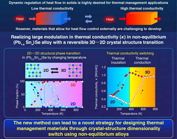
(Nanowerk News) Just as how an electrical switch regulates the flow of electric current, thermal switches can control the flow of heat. These switches serve as thermal control devices and are useful for thermal management applications. For example, they can be used in industries to reduce waste heat, resulting in cost and energy savings.
|
|
These switches require materials whose thermal conductivity (κ) can be modulated to a large extent. This would allow the switch to have an "on" and "off" state depending on the thermal conductivity. However, such materials are rare and challenging to develop, and those that have been developed show only small reversible variations in their κ.
|
 |
| Controlling heat flow in a solid by switching crystal structure dimensionality. (Image: Tokyo Tech)
|
|
Now, in a study published in Advanced Electronic Materials ("Electronic and lattice thermal conductivity switching by 3D−2D crystal structure transition in Nonequilibrium (Pb1−xSnx)Se"), researchers from Tokyo Institute of Technology (Tokyo Tech) and the National Institute for Materials Science, Japan, have taken things to the next level with a material that can achieve a large variation in its κ by changing its crystal structure dimensionality.
|
|
The team achieved this remarkable feat by using a solid solution of lead selenide (PbSe) and tin selenide (SnSe), which can switch between a 3-dimensional (3D) cubic crystal structure and a 2-dimensional (2D) layered crystal structure with changes in temperature.
|
|
In solids, heat is transported by two different processes, namely the vibrations of the crystalline lattice, and the flow of electric charge carriers. Therefore, the thermal conductivity of a solid depends on both the crystal structure and electronic structure.
|
|
In their study, the researchers were able to obtain different κ values in a (Pb0.5>/Sn0.5)Se alloy by changing the crystal structure dimensionality owing to the different arrangements of atoms and band gaps in each crystal structure relative to the other.
|
|
"The material we chose for our study is bulk polycrystals of (Pb0.5>/Sn0.5)Se, which shows a direct phase boundary between the 3D and 2D crystal structures. We achieved this by thermally quenching the high-temperature solid solution phase to room temperature" explains Professor Takayoshi Katase from Tokyo Tech, who was involved with the study.
|
|
The researchers could reversibly switch between the 3D and 2D crystal structure dimensionalities of the (Pb0.5>/Sn0.5)Se polycrystals by simply heating and cooling the material. In the heated state, the material assumed a 3D crystal structure with a metallic electronic structure, which resulted in a high electronic as well as lattice thermal conductivity.
|
|
When cooled, on the other hand, it changed to a 2D crystal structure with a semiconducting electronic structure and a largely reduced κ. At a temperature of 373 K (100 °C), the κ for the 3D phase was observed to be 3.6 times higher than that for the 2D phase.
|
|
This new approach to altering κ could pave the way for the design of more such materials with potential applications in thermal management. "We believe that the present strategy will lead to a novel concept for designing thermal switching material through changing the crystal-structure dimensionality across non-equilibrium phase boundaries," says Prof. Katase.
|

