| Oct 14, 2022 |
Clarification of material properties for clearly better displays(Nanowerk News) All displays consist of a lattice of tiny dots of light, called pixels, the brightness of which can be individually controlled. The total number of pixels—and therefore, the resolution and display size—is limited by how many of these pixels can be addressed within a given fraction of a second. Therefore, display manufacturers try to use in the pixel control units materials that exhibit a very high "electron mobility", which is a measure for how quickly current will start to flow through such a control unit as a response to voltage being applied—and thus, how "quick" the pixel is. |
| A new material called "ITZO" (for its constituent elements indium, tin, zinc and oxygen) promises to be up to seven times faster than the current state-of-the-art material. However, it has not been clear where this improvement comes from, hampering its adoption for industrial applications. |
| Hokkaido University material scientist Hiromichi Ohta and his team used their unique measurement technique to clarify this point. In their recent paper published in the journal Applied Electronic Materials ("Thermopower Modulation Analyses of High-Mobility Transparent Amorphous Oxide Semiconductor Thin-Film Transistors"), they showed that the higher electron mobility results from the unusual fact that in ITZO films of sufficient thickness, free charges accumulate at the interface with the carrier material and thus enable passing-through electrons to travel through the bulk of the material unhindered. |
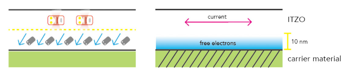 |
| Conceptual drawing explaining the high electron mobility of ITZO material. During a motorway emergency, cars move to one side to clear the path for emergency vehicles. In a similar fashion, free electrons move to the 10-nm-thick interface of the ITZO material with the carrier material and thus create a large bulk where current can flow unhindered. (Image: Ikumi Hatakeyama) |
| The unique ability of the group around Ohta comes down to a very simple formula: The electron mobility is proportional to the free travel time of the charge carriers—electrons in this case—divided by their effective mass. And while the measurement of the electron mobility itself is a relatively standard technique, effective mass and free travel time cannot be measured as easily, and therefore it is difficult to tell what factor is responsible for the electron mobility. |
| But by measuring how the electric field inside the material changes in response to an applied magnetic field as well as to a temperature gradient, Ohta's team could deduce the effective mass of the electrons—and then calculate the free travel time, as well. |
| It turns out that both the effective mass is significantly smaller than in current state-of-the-art materials and the free travel time is much higher and, therefore, both factors contribute to the higher electron mobility. |
| In addition, by observing how their results depend on the thickness of the ITZO material, they could deduce how interface and bulk of the material contribute to these effects. |
| Ohta explains the significance of this analysis: "Using the knowledge we gained from this study, we may in the future design other transparent oxide semiconductor thin-film transistors with different chemical compositions that exhibit even better electron mobility properties." Thus, this study is a major step towards the next generation of ultra high-resolution displays. |
| Source: Hokkaido University |

