| Nov 03, 2022 |
Novel nanowire fabrication technique paves way for next generation spintronics(Nanowerk News) As our world modernizes faster than ever before, there is an ever-growing need for better and faster electronics and computers. Spintronics is a new system which uses the spin of an electron, in addition to the charge state, to encode data, making the entire system faster and more efficient. Ferromagnetic nanowires with high coercivity (resistance to changes in magnetization) are required to realize the potential of spintronics. Especially L10-ordered (a type of crystal structure) cobalt–platinum (CoPt) nanowires. |
| Conventional fabrication processes for L10-ordered nanowires involve heat treatment to improve the physical and chemical properties of the material, a process called annealing on the crystal substrate; the transfer of a pattern onto the substrate through lithography; and finally the chemical removal of layers through a process called etching. Eliminating the etching process by directly fabricating nanowires onto the silicon substrate would lead to a marked improvement in the fabrication of spintronic devices. However, when directly fabricated nanowires are subjected to annealing, they tend to transform into droplets as a result of the internal stresses in the wire. |
| Recently, a team of researchers led by Professor Yutaka Majima from the Tokyo Institute of Technology have found a solution to the problem. The team reported a new fabrication process to make L10-ordered CoPt nanowires on silicon/silicon dioxide (Si/SiO2) substrates. |
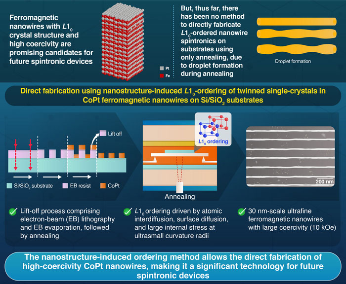 |
| Novel method for direct fabrication of ferromagnetic nanowires on silicon substrates. (Image: Tokyo Tech) |
| Talking about their research, published in Nanoscale Advances ("Nanostructure-induced L10 -ordering of twinned single crystals in CoPt ferromagnetic nanowires"), Prof. Majima says, “Our nanostructure-induced ordering method allows the direct fabrication of ultrafine L10-ordered CoPt nanowires with the narrow widths of 30nm scale required for spintronics. This fabrication method could further be applied to other L10-ordered ferromagnetic materials such as iron–platinum and iron–palladium compounds.” |
| In this study, the researchers first coated a Si/SiO2 substrate with a material called a ‘resist’ and subjected it to electron beam lithography and evaporation to create a stencil for the nanowires. Then then deposited a multilayer of CoPt on the substrate. The deposited sampled were then ‘lifted-off’, leaving behind CoPt nanowires. These nanowires were then subjected to high temperature annealing. The researchers also examined the fabricated nanowires using several characterization techniques. |
| They found that the nanowires took on L10-ordering during the annealing process. This transformation was induced by atomic interdiffusion, surface diffusion, and extremely large internal stress at the ultrasmall 10 nm scale curvature radii of the nanowires. They also found that the nanowires exhibited a large coercivity of 10 kiloOersteds (kOe). |
| According to Prof. Majima, “The internal stresses on the nanostructure here induce the L10-ordering. This is a different mechanism than in previous studies. We are hopeful that this discovery will open up a new field of research called ‘nanostructure-induced materials science and engineering.’” |
| The wide applicability and convenience of the novel fabrication technique is sure to make a significant contribution to the field of spintronics research. |
| Source: Tokyo Institute of Technology |

