| Feb 25, 2023 |
Researchers create single-photon emitters exactly where they are needed
(Nanowerk News) In the very near future, quantum computers are expected to revolutionize the way we compute, with new approaches to database searches, AI systems, simulations and more. But to achieve such novel quantum technology applications, photonic integrated circuits which can effectively control photonic quantum states – the so-called qubits – are needed.
|
|
Physicists from the Helmholtz-Zentrum Dresden-Rossendorf (HZDR), TU Dresden and Leibniz-Institut für Kristallzüchtung (IKZ) have made a breakthrough in this effort: for the first time, they demonstrated the controlled creation of single-photon emitters in silicon at the nanoscale, as they report in Nature Communications ("Wafer-scale nanofabrication of telecom single-photon emitters in silicon").
|
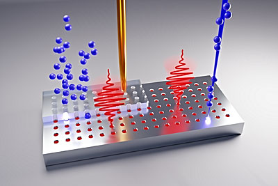 |
| Controlled generation of single-photon emitters in silicon (red) by broad-beam implantation of ions (blue) through a lithographically defined mask (left) and by a scanned focused ion beam (right). Symbolically shown: the emission of two single photons at locations defined for this purpose by the process. In the background: An electron beam creates holes in the lithographic mask made of acrylate. (Image: M. Hollenbach, B. Schröder, HZDR)
|
|
Photonic integrated circuits, or in short, PICs, utilize particles of light, better known as photons, as opposed to electrons that run in electronic integrated circuits. The main difference between the two: A photonic integrated circuit provides functions for information signals imposed on optical wavelengths typically in the near infrared spectrum.
|
|
“Actually, these PICs with many integrated photonic components are able to generate, route, process and detect light on a single chip”, says Dr. Georgy Astakhov, Head of Quantum Technologies at HZDR's Institute of Ion Beam Physics and Materials Research, and adds: “This modality is poised to play a key role in upcoming future technology, such as quantum computing. And PICs will lead the way.”
|
|
Before, quantum photonics experiments were notorious for the massive use of “bulk optics” distributed across the optical table and occupying the entire lab. Now, photonic chips are radically changing this landscape. Miniaturization, stability and suitability for mass production might turn them into the workhorse of modern-day quantum photonics.
|
From random to control mode
|
|
Monolithic integration of single-photon sources in a controllable way would give a resource-efficient route to implement millions of photonic qubits in PICs. To run quantum computation protocols, these photons must be indistinguishable. With this, industrial-scale photonic quantum processor production would become feasible.
|
|
However, the currently established fabrication method stands in the way of the compatibility of this promising concept with today's semiconductor technology.
|
|
In a first attempt reported about two years ago, the researchers were already able to generate single photons on a silicon wafer, but only in a random and non-scalable way. Since then, they have come far. “Now, we show how focused ion beams from liquid metal alloy ion sources are used to place single-photon emitters at desired positions on the wafer while obtaining a high creation yield and high spectral quality”, says Dr. Nico Klingner, physicist.
|
|
Furthermore, the scientists at HZDR subjected the same single-photon emitters to a rigorous material testing program: After several cooling-down and warming-up cycles, they did not observe any degradation of their optical properties. These findings meet the preconditions required for mass production later on.
|
|
To translate this achievement into a widespread technology, and allow for wafer-scale engineering of individual photon emitters on the atomic scale compatible with established foundry manufacturing, the team implemented broad-beam implantation in a commercial implanter through a lithographically defined mask.
|
|
“This work really allowed us to take advantage of the state-of-the-art silicon processing cleanroom and electron beam lithography machines at the Nano Fabrication facility Rossendorf”, explains Dr. Ciarán Fowley, Cleanroom group leader and Head of Nanofabrication and Analysis.
|
|
Using both methods, the team can create dozens of telecom single-photon emitters at predefined locations with a spatial accuracy of about 50 nm. They emit in the strategically important telecommunication O-band and exhibit stable operation over days under continuous-wave excitation.
|
|
The scientists are convinced that the realization of controllable fabrication of single-photon emitters in silicon makes them a highly promising candidate for photonic quantum technologies, with a fabrication pathway compatible with very large-scale integration. These single-photon emitters are now technologically ready for production in semiconductor fabs and incorporation into the existing telecommunication infrastructure.
|

