| Jan 29, 2024 |
Researchers developed a new self-assembly method to fabricate multilayered 2D nanosheets
(Nanowerk News) As electronic devices get smaller, the materials needed to create them get smaller as well. Nanoscience is the study of extremely small materials that find uses in energy storage, electronics, health and safety applications and more.
|
|
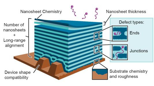
Now a team led by the U.S. Department of Energy’s (DOE) Lawrence Berkeley National Laboratory has developed a new self-assembly method to fabricate multilayered 2D nanosheets. A nanosheet is an extremely small, lasagna-like material made of ultrathin layers of polymers and nanoparticles.
|
|
These nanosheets have significantly reduced the number of defects compared with previous methods, which will extend the shelf life of some consumer electronics. Because the nanosheets synthesized by this new method are recyclable, this method could also enable a sustainable manufacturing approach that reduces the number of parts on an electronic device that need to be dumped into landfills.
|
|
The team is the first to successfully develop a multipurpose, high-performance barrier material from self-assembling nanosheets. Researchers made use of the Advanced Photon Source (APS), a DOE Office of Science user facility at DOE’s Argonne National Laboratory.
|
|
The breakthrough was reported in the journal Nature ("Functional composites by programming entropy-driven nanosheet growth").
|
 |
| Artist’s rendition of stacked nanosheets for high-performance barrier coating, which requires a minimization of defects. (Image: Qingteng Zhang/Argonne National Laboratory)
|
|
“Our work overcomes a longstanding hurdle in nanoscience — scaling up nanomaterial synthesis into useful materials for manufacturing and commercial applications,” said Berkeley Lab senior scientist Ting Xu, the principal investigator who led the study. “It’s really exciting because this has been decades in the making.”
|
|
One challenge in leveraging nanoscience to create functional materials is that many small pieces need to come together. This is so that the nanomaterial can grow large enough to be useful. While stacking nanosheets is one of the simplest ways to grow nanomaterials into a product, “stacking defects” — gaps between the nanosheets — are unavoidable when working with existing nanosheets.
|
|
“If you visualize building a 3D structure from thin, flat tiles, you’ll have layers up the height of the structure. But you’ll also have gaps throughout each layer wherever two tiles meet,” said first author Emma Vargo, a former graduate student researcher and now a postdoctoral scholar at Berkeley Lab. “It’s tempting to reduce the number of gaps by making the tiles bigger, but they become harder to work with,” Vargo said.
|
|
The new nanosheet material overcomes the problem of stacking defects by skipping the serial stacked sheet approach altogether. Instead, the team mixed blends of materials that are known to self-assemble into small particles. They used alternating layers of the component materials, suspended in a solvent.
|
|
Experiments at the Spallation Neutron Source, a DOE Office of Science user facility at DOE’s Oak Ridge National Laboratory, helped the researchers understand the early, coarse stages of the blends’ self-assembly. As the solvent evaporates, the small particles coalesce and spontaneously organize, coarsely templating layers. They then solidify into dense nanosheets. In this way, the ordered layers form simultaneously rather than being stacked one by one in a serial process. The small pieces only need to move short distances to get organized and close gaps. This avoids the problems of moving larger “tiles” and the inevitable gaps between them.
|
|
The researchers predicted that the complex blend used for the current study would have two ideal properties. They also expected that the new nanosheet system would be minimally affected by different surface chemistries. This, they reasoned, would allow the same blend to form a protective barrier on a variety of surfaces, such as the glass screen of an electronic device, or a polyester mask.
|
|
To test the performance of the material as a barrier coating in several different applications, the researchers enlisted the help of some of the nation’s best research facilities.
|
|
During experiments at the APS, the researchers studied how a mixture of polymers, organic small molecules and nanoparticles forms a film on the inner wall of a quartz capillary tube, when the solvent slowly evaporates in dry air.
|
|
“Thanks to the brilliant X-rays produced by the APS and the sophisticated X-ray detector stationed at Beamline 8-ID-I, we were able to map out how each component comes together across a wide range of length scales,” said Argonne scientist Qingteng Zhang, a co-author on the paper.
|
|
Now that they’ve successfully demonstrated how to easily synthesize a versatile functional material for various industrial applications from a single nanomaterial, the researchers plan to finetune the material’s recyclability. They’ll also add color tunability (it currently comes in blue) to its repertoire.
|
|
The APS is undergoing a comprehensive upgrade. When complete, the upgraded APS will enable probing of the self-assembly of the nanoparticles from nanoscopic to device scale, starting at the very beginning of the self-assembly process.
|

