| Jul 15, 2025 |
Realizing on-site carbon nanotube photo-thermoelectric imaging
Chemically enriched photo-thermoelectric imagers built from semiconducting carbon nanotube films show improved signal response and reduced noise, enabling more efficient remote and on-site inspections.
(Nanowerk News) Researchers at Chuo University in Japan, led by Assistant Professor Kou Li, have developed a new class of photo-thermoelectric (PTE) imagers using specially treated carbon nanotube (CNT) films. These imagers show significant improvements in both signal strength and noise reduction, making them highly effective for remote and on-site inspections.
|
|
The work, recently published in Communications Materials ("A chemically enriched, repeatedly deformable, and self-recoverable broadband wireless imager sheet"), addresses long-standing challenges in using PTE imagers for industrial quality control and non-destructive testing.
|
 |
| Device Concept. Remote-Controlled Non-destructive Testing Image Sensor Using Doped s-CNT. (Image: Chuo University)
|
|
Traditional CNT-based PTE imagers play an important role in detecting electromagnetic waves across a broad range of frequencies. They’re particularly valued for their ability to function without damaging the objects under inspection. However, these systems have historically struggled with weak signal intensities—typically limited to a few millivolts—which restricts their compatibility with small, wireless data loggers. These limitations have made it difficult to use them in practical, portable setups for field applications.
|
|
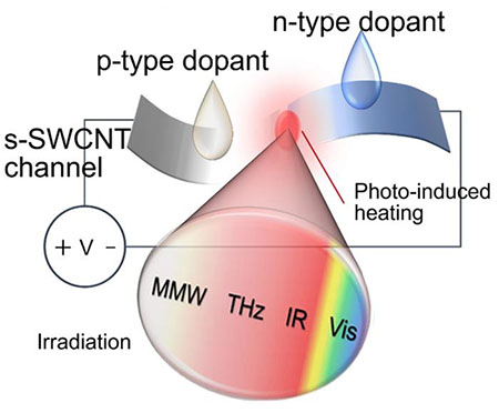
The new approach uses CNT films that are chemically enriched to consist predominantly of semiconducting carbon nanotubes. This change alone boosts thermoelectric response compared to earlier mixtures that included semi-metallic types. The researchers went further by introducing chemical carrier doping—specifically p-type and n-type treatments—to fine-tune the material’s electronic properties. This dual-doping method addresses the problem of high intrinsic noise that has historically limited the sensitivity of such systems.
|
|
As a result, the improved CNT-based imagers deliver performance gains up to 4,060 times greater in terms of thermoelectric conversion efficiency. They achieve a signal response level ranging from a few to several tens of millivolts, comfortably surpassing the threshold needed to pair with compact wireless circuits. In practical terms, this makes them viable for field-ready applications that require minimal hardware and real-time data transmission.
|
|
Despite the technical improvements, these imagers retain key features of earlier CNT devices, including the ability to detect light across an ultrabroadband spectrum—from millimeter waves to visible light—and remain functional under repeated physical deformation. With a noise sensitivity as low as 5 picowatts per square root hertz, they offer a rare combination of flexibility, range, and responsiveness.
|
|
This innovation comes at a time when industries increasingly rely on fast, reliable, and portable systems to inspect complex components during manufacturing and distribution. Conventional imagers, with their low signal intensities, have fallen short of integrating seamlessly with wireless systems, especially for real-time, on-site testing. The new chemically enriched PTE imagers overcome this mismatch, allowing for remote, omnidirectional, and multi-wavelength inspections—even of aerial objects—using lightweight, palm-sized circuits.
|
|
By solving the dual problem of signal strength and noise, the Chuo University team has opened the door to a new generation of compact, high-performance photo-imaging tools. These could play a critical role in transforming non-destructive testing and quality assurance across a wide range of sectors, from aerospace to civil infrastructure.
|

