| Posted: May 14, 2009 |
Scientists have directly measured the unusual energy spectrum of graphene |
|
(Nanowerk News) Applying innovative measurement techniques, researchers from the Georgia Institute of Technology and the National Institute of Standards and Technology (NIST) have directly measured the unusual energy spectrum of graphene, a technologically promising, two-dimensional form of carbon that has tantalized and puzzled scientists since its discovery in 2004.
|
|
Published in this week’s issue of Science (D.L. Miller, K.D. Kubista, G.M. Rutter, M. Ruan, W.A. de Heer, P.N. First and J.A. Stroscio. Observing the quantization of zero mass carriers in graphene. Science. May 15, 2009.), their work adds new detail to help explain the unusual physical phenomena and properties associated with graphene, a single layer of carbon atoms arrayed in a repeating, honeycomb-like arrangement.
|
|
Graphene’s exotic behaviors present intriguing prospects for future technologies, including high-speed, graphene-based electronics that might replace today’s silicon-based integrated circuits and other devices. Even at room temperature, electrons in graphene are more than 100 times more mobile than in silicon.
|
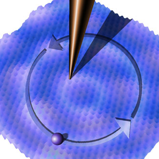 |
| Drawing represents a probe scanning and mapping the atomic contours of graphene, a single layer of carbon atoms arranged in a honeycomb-like array. Simultaneously applying a magnetic field causes electrons (ball) to organize in circular orbits, like a dog chasing its tail. Orbits hold clues to the material’s exotic properties. (Image: Kubista, Georgia Institute of Technology)
|
|
Graphene apparently owes this enhanced mobility to the curious fact that its electrons and other carriers of electric charges behave as though they do not have mass. In conventional materials, the speed of electrons is related to their energy, but not in graphene. Although they do not approach the speed of light, the unbound electrons in graphene behave much like photons, massless particles of light that also move at a speed independent of their energy.
|
|
This weird massless behavior is associated with other strangeness. When ordinary conductors are put in a strong magnetic field, charge carriers such as electrons begin moving in circular orbits that are constrained to discrete, equally spaced energy levels. In graphene these levels are known to be unevenly spaced because of the “massless” electrons.
|
|
The Georgia Tech/NIST team tracked these massless electrons in action, using a specialized NIST instrument to zoom in on the graphene layer at a billion times magnification, tracking the electronic states while at the same time applying high magnetic fields. The custom-built, ultra-low-temperature and ultra-high-vacuum scanning tunneling microscope allowed them to sweep an adjustable magnetic field across graphene samples prepared at Georgia Tech, observing and mapping the peculiar non-uniform spacing among discrete energy levels that form when the material is exposed to magnetic fields.
|
|
|
|
The team developed a high-resolution map of the distribution of energy levels in graphene. In contrast to metals and other conducting materials, where the distance from one energy peak to the next is uniformly equal, this spacing is uneven in graphene.
|
|
The researchers also probed and spatially mapped graphene’s hallmark “zero energy state,” a curious phenomenon where the material has no electrical carriers until a magnetic field is applied.
|
|
The measurements also indicated that layers of graphene grown and then heated on a substrate of silicon-carbide behave as individual, isolated, two-dimensional sheets. On the basis of the results, the researchers suggest that graphene layers are uncoupled from adjacent layers because they stack in different rotational orientations. This finding may point the way to manufacturing methods for making large, uniform batches of graphene for a new carbon-based electronics.
|

