| Posted: October 30, 2007 |
World's most complex silicon phased-array chip developed at UC-San Diego |
|
(Nanowerk News) UC San Diego electrical engineers have developed the world’s most complex “phased array” – or radio frequency integrated circuit. This DARPA-funded advance is expected to find its way into U.S. defense satellite communication and radar systems. In addition, the innovations in this chip design will likely spill over into commercial applications, such as automotive satellite systems for direct broadcast TV, and new methods for high speed wireless data transfer.
|
|
“This is the first 16 element phased array chip that can send at 30-50 GHz. The uniformity and low coupling between the elements, the low current consumption and the small size – it is just 3.2 by 2.6 square millimeters – are all unprecedented. As a whole system, there are many many firsts,” said Gabriel Rebeiz, the electrical engineering professor from the UCSD Jacobs School of Engineering leading the project. The work was done by two graduate students, Kwang-Jin Koh and Jason May, both at the Electrical and Computer Engineering Department (ECE) at UCSD. Rebeiz presented the new chip at DARPA TEAM Meeting, August 28-29, 2007 in Chicago, Illinois. Additional details of the chip will be submitted to an academic journal later this year.
|
|
This chip – the UCSD DARPA Smart Q-Band 4x4 Array Transmitter – is strictly a transmitter. “We are working on a chip that can do a transmit and receive function,” said Rebeiz.
|
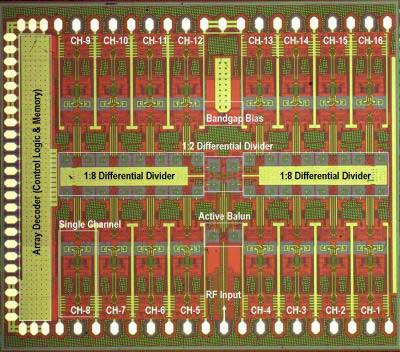 |
| The UCSD DARPA Smart Q-Band 4x4 Array Transmitter, the world's most complex silicon phased-array chip was developed in the lab of UC-San Diego electrical engineering professor Gabriel Rebeiz. (Image: Gabriel Rebeiz / UC San Diego)
|
|
“This compact beamforming chip will enable a breakthrough in size, weight, performance and cost in next-generation phased arrays for millimeter-wave military sensor and communication systems,” DARPA officials wrote in a statement.
|
|
“DARPA has funded us to try to get everything on a single silicon chip – which would reduce the cost of phased arrays tremendously. In large quantities, this new chip would cost a few dollars to manufacture. Obviously, this is only the transmitter. You still need the receiver but one can easily build the receiver chip based on the designs available in the transmitter chip. Our work addresses the most costly part of the phased array – the 16:1 divider, phase shifters, amplitude controllers and the uniformity and isolation between channels,” said Rebeiz.
|
|
The chip also contains all the CMOS digital circuits necessary for complete digital control of the phased array, and was done using the commercial Jazz SBC18HX process. This is a first and greatly reduces the fabrication complexity of the phased array. The chip has been designed for use at the defense satellite communications frequency – the Q-band - which goes from 40 to 50 GHz.
|
|
“If you take the same design and move it to the 24 or 60 GHz range, you can use it for commercial terrestrial communications,” said Rebeiz who is also a lead on a separate project, funded by Intel and a UC-Discovery Grant, to create silicon CMOS phased array chips that could be embedded into laptops and serve as high speed data transfer tools.
|
|
The Intel project is a collaboration between Rebeiz, Larry Larson and Ian Galton – all electrical engineering professors at the UCSD Jacobs School of Engineering. Larson also serves as the chair of the Department of Electrical and Computer Engineering.
|
|
“If you wanted to download a large movie file, a base station could find you, zoom onto you, and direct a beam to your receiver chip. This could enable data transfer of hundreds of gigabytes of information very quickly, and without connecting a cable or adhering to the alignment requirements of wireless optical data transfer,” explained Rebeiz who estimated that this kind of system could be available in as little as three years.
|
|
Phased Array Background Information:
|
|
Phased arrays have been around for more than half a century. They are groups of antennas in which the relative phases of the signals that feed them are varied so that the effective radiation pattern of the array is reinforced in a particular direction and suppressed in undesired directions. This property – combined with the fact that radio waves can pass through clouds and most other materials that stymie optical communication systems – has led engineers to use phased arrays for satellite communications, and for detecting incoming airplanes, ships and missiles.
|
|
Some phased arrays are larger than highway billboards and the most powerful – used as sophisticated radar, surveillance and communications systems for military aircraft and ships – can cost hundreds of millions of dollars. The high cost has prevented significant spread beyond military and high-end satellite communication applications. Engineers are now working to miniaturize them and fully integrate them into silicon-based electronic systems for both military and commercial applications.
|
|
The new UCSD chip packs 16 channels into a 3.2 by 2.6 mm² chip. The input signal is divided on-chip into 16 different paths with equal amplitude and phase using an innovative design, and the phase and gain of each of the 16 channels is controlled electronically to direct the antenna pattern (beam) into a specific direction.
|
|
By manipulating the phase, you can steer the beam electronically in nanoseconds. With the amplitude, you control the width of the beam, which is critical, for example, when you send information to from one satellite to another but you don’t want the signal to reach any nearby satellites. And with amplitude and phase control, you can synthesize deep nulls in the antenna pattern so as to greatly reduce the effect of interfering signals from neighboring transmitters.
|
|
Source: University of California - San Diego
|

