| Jul 03, 2012 |
Metallized DNA as future electronic components |
| (Nanowerk News) Our electronic devices are getting smaller and smaller while doing more and more. Using conventional materials, we will soon reach the practical limit. The electronics of tomorrow require alternatives, such as nanowires made of DNA that can serve as conductive paths and nanotransistors for miniature circuits. In the journal Angewandte Chemie ("Surface “Click” Reaction of DNA followed by Directed Metalization for the Construction of Contactable Conducting Nanostructures"), German scientists have now described a new method for the production of stable, conducting DNA nanowires. |
 |
| A difunctional DNA template is first immobilized on a functionalized substrate by a copper-catalyzed reaction, modified with silver nucleation centers, and then metalized by gold deposition. The diameter of the resulting metallically conductive nanowires can be adjusted. |
| DNA is more than a carrier of genetic information; it is also an interesting building material for nanotechnology. This is because of its extraordinary self-organizational properties. DNA is thus often used as a “mold” for the production of nanoscale structures. Its use in the assembly of electronic circuits is hampered by the fact that DNA is a very poor conductor of electricity. One way to get around this is by depositing metal onto the DNA strands. |
| Scientists at the RWTH Aachen and the University of Munich have now developed a new strategy for the controlled production and metallization of DNA nanostructures. Led by Ulrich Simon, the team used a DNA strand consisting of an immobilization sequence and a metallization sequence. Several such strands are strung together so that the resulting DNA is made of alternating sequences. |
| The immobilization sequence contains alkyne groups. These allow the DNA to be snapped into place on a silicon wafer coated with azide groups in what is known as a “click” reaction. The other DNA segment has two tasks: it is equipped with functional groups that cause the aggregation of silver particles and can also attach DNA strands to each other. |
| The DNA strands are stretched, deposited onto the wafers, and attached by the “click” reaction. During the subsequent metallization with silver particles, neighboring strands are simultaneously cross-linked to form multistrands. These have significantly higher structural stability than single strands. In the future, this method could also be used to integrate the DNA strands into programmable DNA architectures to allow for the positioning and binding of complex structures on prestructured substrates. |
| Deposition of the silver particles does not complete the metallization process. In a second step, which resembles the development of photographs, gold from a solution can be deposited onto the silver particles. Changing the duration of the gold deposition process allows for variation of the diameter of the resulting nanowires. |
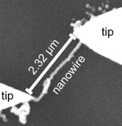
| This new method allowed the scientists to obtain micrometer-long, electrically contactable nanowires that have potential for development into further miniaturized circuits. |
| Source: Wiley |

