| Jul 10, 2012 |
Ferroelectricity on the nanoscale
|
|
(Nanowerk News) Promising news for those who relish the prospects of a one-inch chip storing multiple terabytes of data, some clarity has been brought to the here-to-fore confusing physics of ferroelectric nanomaterials. A multi-institutional team of researchers, led by scientists at the U.S. Department of Energy (DOE)’s Lawrence Berkeley National Laboratory (Berkeley Lab) has provided the first atomic-scale insights into the ferroelectric properties of nanocrystals. This information will be critical for development of the next generation of nonvolatile data storage devices.
|
|
Working with the world’s most powerful transmission electron microscope, the researchers mapped the ferroelectric structural distortions in nanocrystals of germanium telluride, a semiconductor, and barium titanate, an insulator. This data was then combined with data from electron holographic polarization imaging to yield detailed information on the polarization structures and scaling limits of ferroelectric order on the nanoscale.
|
|
“As we scale down our device technology from the microscale to the nanoscale, we need a better understanding of how critical material properties, such as ferroelectric behavior, are impacted,” says Paul Alivisatos, director of Berkeley Lab and one of the principal investigators in this research. “Our results provide a pathway to unraveling the fundamental physics of nanoscale ferroelectricity at the smallest possible size scales.”
|
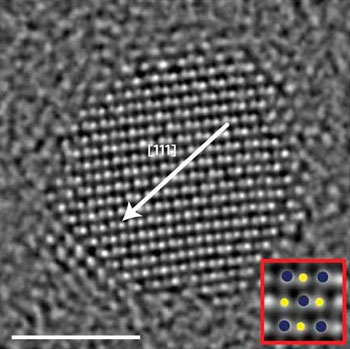 |
| Atomic-resolution images of germanium telluride nanoparticles from Berkeley Lab’s TEAM I electron microscope, and electron holographic images of barium titanate nanoparticles (below) from BNL yielded the first detailed experimental information on ferroelectric order at the nanoscale.
|
|
Alivisatos, who is also the Larry and Diane Bock Professor of Nanotechnology at the University of California (UC) Berkeley, is a corresponding author of a paper describing this work in the journal Nature Materials titled “Ferroelectric order in individual nanometrescale Crystals”. The other corresponding author is Ramamoorthy Ramesh, a senior scientist with Berkeley Lab’s Materials Sciences Division and the Plato Malozemoff Professor of Materials Science and Physics for UC Berkeley.
|
|
Ferroelectricity is the property by which materials can be electrically polarized, meaning they will be oriented in favor of either a positive or negative electrical charge. This polarization can be flipped with the application of an external electrical field, a property that could be exploited for nonvolatile data storage, similar to the use of ferromagnetic materials today but using much smaller, far more densely packed devices.
|
|
“Although much progress has been made towards understanding nanoscale photophysical magnetic and other functional properties, understanding the basic physics of ferroelectric nanomaterials remains far less advanced,” says co-principal investigator Ramesh, who attributes contradicting reports on nanoscale ferroelectricity in part to the lack of high-quality, nanocrystals of ferroelectric materials that feature well-defined sizes, shapes and surfaces.
|
|
“Another problem has been the reliance on ensemble measurements rather than single particle techniques,” he says. “Statistical-average measurement techniques tend to obscure the physical mechanisms responsible for profound changes in ferroelectric behavior within individual nanocrystals.”
|
|
The Berkeley Lab-led research team was able to map ferroelectric structural distortions within individual nanocrystals thanks to the unprecedented capabilities of TEAM I, which is housed at Berkeley Lab’s National Center for Electron Microscopy (NCEM). TEAM stands for “Transmission Electron Aberration-corrected Microscope.” TEAM I can resolve images of structures with dimensions as small as one half-angstrom – less than the diameter of a single hydrogen atom.
|
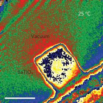 |
| Electron holographic images of barium titanate nanoparticles.
|
|
The maps produced at TEAM I of ferroelectric distortion patterns within the highly conducting germanium telluride nanocrystals were then compared with electron holography studies of insulating nanocubes of barium titanate, which were carried out by collaborators at Brookhaven National Laboratory (BNL).
|
|
“Electron holography is an interferometry technique using coherent electron waves,” said BNL physicist and co-author of the Nature Materials paper Myung-Geun Han. “Firing focused electron waves through the ferroelectric sample creates what’s called a phase-shift, or an interference pattern that reveals details of the targeted structure. This produces an electron hologram, which we can use to directly see local electric fields of individual ferroelectric nanoparticles.”
|
|
These combined studies enabled the independent examination of depolarizing field and surface structure influences and thereby enabled the research team to identify the fundamental factors governing the nature of the ferroelectric polarized state at finite dimensions. The results indicate that a monodomain ferroelectric state with linearly ordered polarization remains stable in these nanocrystals down to dimensions of less than 10 nanometers. Also, room-temperature polarization flipping was demonstrated down to dimensions of about five nanometers. Below this threshold, ferroelectric behavior disappeared. This indicates that five nanometers is likely a size limit for data storage applications, the authors state.
|
|
“We also showed that ferroelectric coherence is facilitated in part by control of particle morphology, which along with electrostatic boundary conditions is found to determine the spatial extent of cooperative ferroelectric distortions,” Ramesh says. “Taken together, our results provide a glimpse of the structural and electrical manifestations of ferroelectricity down to its ultimate limits.”
|

