| Dec 14, 2012 |
Nanocrystals not small enough to avoid defects
|
|
(Nanowerk News) Nanocrystals as protective coatings for advanced gas turbine and jet engines are receiving a lot of attention for their many advantageous mechanical properties, including their resistance to stress. However, contrary to computer simulations, the tiny size of nanocrystals apparently does not safeguard them from defects.
|
|
In a study by researchers with the U.S. Department of Energy (DOE)’s Lawrence Berkeley National Laboratory (Berkeley Lab)and collaborators from multiple institutions, nanocrystals of nickel subjected to high pressure continued to suffer dislocation-mediated plastic deformation even when the crystals were only three nanometers in size. These experimental findings, which were carried out at Berkeley Lab’s Advanced Light Source (ALS), a premier source of X-rays and ultraviolet light for scientific research, show that dislocations can form in the finest of nanocrystals when stress is applied.
|
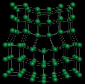 |
| Stress-induced deformation of nanocrystalline nickel reflects the dislocation activity observed by researchers at Berkeley Lab’s Advanced Light Source using a radial diamond-anvil-cell X-ray diffraction experimental station.
|
|
“We cannot ignore or underestimate the role of dislocations – defects or irregularities – in fine nanocrystals as external stress can change the entire picture,” says Bin Chen, a materials scientist with the ALS Experimental Systems Group who led this research. “Our results demonstrate that dislocation-mediated deformation persists to smaller crystal sizes than anticipated, primarily because computer models have not given enough consideration to the effects of external stress and grain boundaries.”
|
|
Chen is the lead and corresponding author of a paper in Science describing this work. The paper is titled “Texture of Nanocrystalline Nickel: Probing the Lower Size Limit of Dislocation Activity”. Co-authoring this paper were Katie Lutker, Selva Vennila Raju, Jinyuan Yan, Waruntorn Kanitpanyacharoen, Jialin Lei, Shizhong Yang, Hans-Rudolf Wenk, Ho-kwang Mao and Quentin Williams.
|
|
Plastic deformation is a permanent change in the shape or size of a material as the result of an applied stress. The likelihood of plastic deformation increases with the presence of dislocations – defects or irregularities – within the material’s structure. Most materials are made up of small crystals, called “grains,” and what happens at the boundaries between these grains is critical to material properties. Based on computer simulations and electron microscopy analysis, the belief has been that dislocation-mediated plastic deformation becomes inactive below a grain size of at least 10 nanometers, and possibly as large as 30 nanometers.
|
|
“The idea was that below a critical length scale, dislocation-mediated deformation activity would give way to grain-boundary sliding, diffusion, and grain rotation,” Chen says. “However, there were many unresolved questions with regards to whether plasticity in ultrafine nanocrystalline grains could still be generated by dislocations and how pressure might affect the deformational regimes.”
|
|
To investigate grain size and pressure effects on the plastic deformation of nanometals, Chen and his colleagues used ALS Beamline 12.2.2, a superconducting bend magnet beamline that supports radial diamond-anvil-cell X-ray diffraction experiments. Chen and his co-authors recorded in situ observations under a range of high pressures of texturing (when the crystalline grains have preferred orientations) in stressed polycrystalline nickel samples featuring grain sizes of 500-, 20- and 3-nanometers.
|
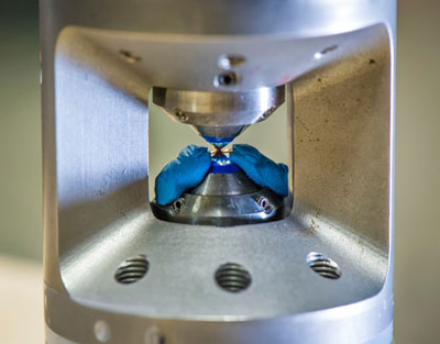 |
| A radial diamond-anvil-cell allows for in situ X-ray diffraction experiments at superbend beamline 12.2.2 of Berkeley Lab’s Advanced Light Source.
|
|
“Substantial texturing was observed at pressures above 3.0 gigapascals for nickel with 500-nanometer grain size and at greater than 11.0 gigapascals for nickel with 20-nanometer grain size,” Chen says. “Surprisingly, texturing was also seen in nickel with 3-nanometer grain size when compressed above 18.5 gigapascals. This tells us that under high external pressures, dislocation activity can be extended down to a few-nanometers-length scale.”
|
|
Chen and his co-authors started with nanocrystalline nickel because its face-center cubic structure remains stable under a wide pressure range. They are now applying their techniques to the study of other nanocrystalline materials, both metals and non-metals.
|

