Showing Spotlights 297 - 304 of 333 in category All (newest first):
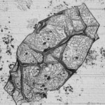
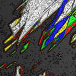
 Graphene has two distinct types of edges produced when it is cut - armchair type or zigzag type - which correspond to the two crystal axis of graphene. These edge types have distinct electronic, magnetic, and chemical properties, and being able to pattern graphene along particular crystallographic directions to leave edges consisting of a single chirality is crucial for the fabrication of graphene nanoribbon and nanoelectronics devices. A widely discussed method for the patterning of graphene is the channelling of graphite by metal nanoparticles in oxidizing or reducing environments. Researchers now report the live nanoscale observation of this channelling process by silver nanoparticles.
Jun 13th, 2011
 Unlike silicon, graphene lacks an electronic band gap - the gap being an energy range that cannot be occupied by electrons - and therefore has no switching capability; which is essential for electronics applications. Opening an energy gap in graphene's electron energy spectrum is therefore a critical prerequisite for instance for creating graphene transistors. That's where strain engineering of graphene comes in. Researchers have discovered that local strain in a graphene sheet can alter its conducting properties. By varying the amount of local strain, transport gaps can be tailored. In new work, researchers present a new and novel mechanism for gap opening in strained graphene via electrostatic gates and show that it can be important also in realistic situations.
Jun 8th, 2011
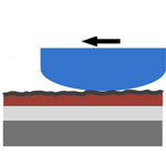 Interaction forces between contact surfaces, such as the adhesion and friction forces, are crucial in many applications at the nanoscale because of the high surface-to-volume ratio of nanomaterials and nanodevices. Over the last decade, various solid lubricant materials, micro/nano patterns, and surface treatment processes have been developed for efficient operation and extended lifetime in MEMS/NEMS applications, and for various fabrication processes such as nanoimprint lithography and transfer printing. From a practical viewpoint, large-area CVD-graphene holds the greatest promise as a solid lubricant because of its excellent scalability and transferability. So far, the tribological characteristics of CVD-graphene at the micro- and nanoscale have not been reported yet. Researchers have now demonstrated the feasibility of using large-area CVD-graphene as a solid lubricant.
May 25th, 2011
 The extremely high electron mobility of graphene - under ideal conditions electrons move through it with roughly 100 times the mobility they have in silicon - combined with its superior strength and the fact that it is nearly transparent (2.3 % of light is absorbed; 97.7 % transmitted), make it an ideal candidate for photovoltaic applications. Recent research suggests, though, that doping is a necessity to harvest the full potential of graphene. The challenge then for researchers is to find suitable fabrication techniques for high-quality graphene flakes that exhibit high charge mobilities. Researchers now present a chemical approach towards non-covalently functionalized graphene, which is generated from vastly available and low-priced natural graphite.
Apr 19th, 2011
 There are already several technologies that potentially allow mass production of graphene sheets; several of them are processing graphene in solution by exfoliating graphite. The general problem with this approach is however that is has been so far impossible to regenerate the undisturbed graphene lattice which was present prior to oxidation as decarboxylation inevitable takes place in the reduction step. In new work, researchers have now demonstrated the first bulk wet chemical exfoliation of graphite in association with an in situ covalent functionalization of intermediately generated graphene. With this novel chemical method, it is now possible to achieve covalently bonded functionalities without mechanical or sonochemical treatment. The covalent functionalization also protects the single-layer graphene from reaggregation and substrate-induced doping.
Mar 25th, 2011
 In the decades-old quest to build artificial muscles, many materials have been investigated with regard to their suitability for actuator application (the ability of a material to reversibly change dimensions under the influence of various stimuli). Recently, hope in obtaining improved artificial muscles was revitalized by the discovery of the extraordinary mechanical and electrical properties of graphene and its chemical derivatives. A new study shows that electrical heating of graphene oxide nanoribbons mats results in reversible generation of 1.6% stress and maximum work capacity of about 40 J/kg, which is similar to that of natural muscle. Unlike previous studies, the team obtained the graphene material by chemical unzipping of multi-walled carbon nanotubes.
Mar 24th, 2011
 An important consideration for practical graphene applications is the fact that the physical characteristics of graphene are strongly dependent on the number of atomic planes, i.e. the properties of few-layer graphene are different from those of single layer graphene. Unfortunately, the one-atom thickness of graphene and its optical transparency make graphene identification and counting the number of atomic planes in few-layer graphene extremely challenging. This complicates the development of industrial-scale applications that would require the handling of large wafers with graphene. Current techniques for counting the number of atomic planes in few-layer graphene samples are either destructive, too complicated, or too slow. Researchers at UC Riverside have now developed a large-scale graphene recognition and quality control technique for industrial applications.
Feb 7th, 2011
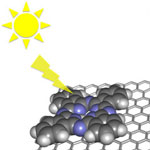
 Graphene is a very interesting nanomaterial with potential for applications in many different fields including nanoelectronics. However, the properties of graphene can vary broadly and depend sensitively on its integration in device structures and the details of its interaction with other materials, such as underlying substrates or gate dielectrics. Unlike other semiconductor electronic devices, where the active layer is buried below the surface and where microscopic details of transport cannot be directly examined, graphene is exposed at a surface and can be directly examined on the atomic scale using scanning tunneling microscopy (STM) and scanning tunneling spectroscopy (STS). New work now provides microscopic details of graphene interaction with a substrate in the most common device structure used so far.
Jan 27th, 2011
 Subscribe to our Nanotechnology Spotlight feed