Showing Spotlights 265 - 272 of 333 in category All (newest first):
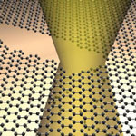 Within graphene research, transmission electron microscopy (TEM) has proven to be an extremely useful and versatile characterization tool. However, the electron beam can interact with the sample leading to its modification during the process. This may be an undesirable effect and measures to avoid this do exist. In other cases, however, electron beam-sample interactions can be useful for nanoengineering or nanomanufacturing. It is therefore crucially important to understand how a material responds to the electron beam and the environment inside a TEM. In new work, researchers have now demonstrated that damage-free sculpting of graphene with condensed electron beams is feasible.
Nov 12th, 2012
 Sensitive electronic devices like cell phones and computers require shielding from electromagnetic interference (EMI). Such shielding - which must be electrically conductive - has traditionally been made of metal, which poses a weight problem in the push to miniaturize and lighten electronics. Previous research has already demonstrated that ultra-lightweight carbon nanostructure-based nanocomposite materials outperform conventional metal shielding due to their light weight, resistance to corrosion, flexibility, and processing advantages. In new work, scientists in Korea have now demonstrated that single-layer graphene is an excellent choice of material for high-performance EMI shielding. They found that CVD-synthesized graphene shows more than seven times greater EMI shielding effectiveness (in terms of dB) than gold film of the same thickness.
Oct 25th, 2012
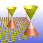
 Controlling the density of electron carriers - which are essential to the operation of electronic devices such as transistors - is achieved by doping conventional three-dimensional semiconductors. But graphene, a semi-metallic layer that is just one atom thick, has properties very different from traditional materials such as silicon. However, the doping of graphene is a key parameter in the development of graphene-based electronics. Researchers have investigated numerous strategies for doping graphene, including attaching organic or metallic molecules to its hexagonal lattice. Now, researchers have managed to dope graphene with light in a way that could lead to more efficient design and manufacture of electronics, as well as novel security and cryptography devices.
Oct 10th, 2012
 The unique energy band structure in graphene allows it to actively respond to photons with ultra-wide spectrum range - from the visible to the infrared - with record strong inter-band transition efficiency. As a consequence, graphene based ultra-fast photonics has been rising fast in various aspects of ultra-fast photonics - an ultra-fast graphene photo-detector with bandwidth exceeding 500 GHz; a broadband graphene optical modulator; a broadband graphene polarizer etc, which all benefit from the material's broadband photonics property. Researchers have now experimentally demonstrated for the first time that graphene, besides its well-known optical saturable absorption, also shows microwave and terahertz saturable absorption. The results lead to the expectation that graphene may show potential applications in microwave photonics.
Oct 2nd, 2012
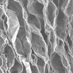
 Researchers have shown that it is possible to use graphene sheets to create a superhydrophobic coating material that shows stable superhydrophobicity under both static as well as dynamic (droplet impact) conditions. They demonstrates a novel macroscopic graphene structure composed of an integrated foam-like network of graphene sheets with well-controlled microscale porosity and roughness. The novel idea here was to grow graphene over a sacrificial nickel foam template and then leech away the nickel, leaving behind a graphene foam with few-layered graphene sheets that comprise the walls of the foam. The foam is then coated with a 200nm layer of Teflon.
Sep 4th, 2012
 Integration of graphene sheets and its functional derivatives into three-dimensional macroscopic structures is drawing much attention since it is an essential step to explore the advanced properties of individual graphene sheets for practical applications, such as chemical filters and electrodes for energy storage devices. However, a major problem in scaling up production of graphene is the tendency of individual graphene sheets to aggregate due to strong van der Waals attraction. Restacking of sheets not only reduces their solution processability, but also compromises their properties such as accessible surface area. A novel approach uses a simple leavening strategy to prepare reduced graphene oxide (rGO) foams with porous and continuous cross-linked structures from freestanding compact graphene oxide layered films. The whole process is more like making graphene "bread". The rGO foams perform excellently as flexible electrode materials for supercapacitors and selective organic absorbents.
Aug 9th, 2012
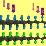 Researchers are putting great efforts into developing techniques to integrate graphene into nanoelectronic devices. Unfortunately, graphene has no band gap - a critical prerequisite for transistors - which essentially restricts its wider applications in nanoelectronics. Among the various techniques developed toward introducing a bandgap in graphene, hydrogenation or fluorination can efficiently solve this problem as they can open a considerable energy gap in the band structure of graphene. However, the experimentally realized fully hydrogenated and fluorinated graphene - namely graphane and fluorographene, respectively - both have a very large energy gap, which constrains their applications in electronics. Thus at present an urgent task is to find a feasible way which could reduce the energy gap of graphane or fluorographene into a desirable range. In new work, researchers have now demonstrated theoretically, using density functional theory computations, that graphane and fluorographene can be paired together through the C-H���F-C hydrogen bonds.
Jul 27th, 2012
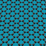
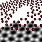 Although graphene in itself has been dubbed the 'magic' material, if it is to be used for practical applications it has to integrated with the other components of possible devices. For instance, to exploit its amazing electron conduction properties, you still need to connect it to the rest of the circuit with contacts, which are typically made out of metal. Understanding how metals interact - chemically and structurally - with graphene is therefore quite important and researchers have published a number of studies on the subject. In a quite unexpected discovery resulting from these observations, researchers have now found that graphene undergoes a self-repairing process to close holes that are caused by metal atoms. They were able to show that nanoscale holes (perhaps a 100 atoms missing or so), etched under an electron beam at room temperature in single-layer graphene sheets as a result of their interaction with metal impurities, heal spontaneously by filling up with either nonhexagon, graphene-like, or perfect hexagon 2D structures.
Jul 18th, 2012
 Subscribe to our Nanotechnology Spotlight feed